


LA000605D © 2007 Navman New Zealand. All rights reserved. Proprietary information and specications subject to change without notice.
2
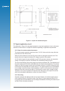
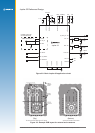
2.1 Electrical connections (SMT pad interface)
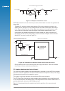
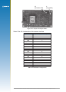
The round hole on the front label side of the chip locates pad A1. The pads are designated
A-F and 1-7. Details of the pad layout and numbering are shown in Figure 2-1.
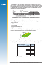
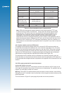
Pad No Pad Names Type Description
A1 RF_IN I RF Input 50 ohm
A2 GND P RF signal ground return
A3 GND P ground
A4 VANT P active antenna power input
A5 GPIO15 I/O reserved
A6 GPIO14 I/O reserved
A7 RF_ON O output to indicate whether the RF section is
enabled (active high)
B1 GND P RF signal ground return
B3 VDD_BB P baseband power supply input for external
regulator build option - DO NOT CONNECT
B4 GPIO4 I/O reserved
B5 GPIO13 I/O reserved
B6 VDD_RTC P RTC power supply input for external regulator
build option - DO NOT CONNECT
B7 GPIO1 I/O reserved
C1 GND P ground
C2 TCXO_IN I TCXO input for external TCXO build option
- DO NOT CONNECT
C4 BOOT I active high to download ash rmware
C5 LNA _EN O external antenna enable, active high
D2 FACTORY USE ONLY reserved
D4 N_GPS_FIX O active low when 2D or 3D x data
available
D5 RXA I CMOS level asynchronous input for UART A
D7 TXA O CMOS level asynchronous output for UART A
E1 GND P ground
E2 GND P ground
E4 GPIO2 I/O reserved
E5 N_RESET I master reset, active low
E6 RXB I CMOS level asynchronous input for UART B
E7 1PPS O 1 pulse per second output 1µs wide
F1 PWRIN P 3.0 - 3.6 V main power supply input
F2 VBATT P 1.9 - 3.6 V backup battery input
F3 VCC_RF P RF power supply output for external regulator
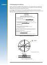
option. Connect as per application circuit.
- Figure 2-2
F4 WAKEUP I Push-to-Fix wake-up, active high
F5 N_WAKEUP O low output indicates baseband is powered up
- DO NOT CONNECT
F6 TXB O CMOS level asynchronous output for UART B
F7 ECLK I external clock input, not used
Table 2-1: Jupiter 32 Module pad functions