


LA000605D © 2007 Navman New Zealand. All rights reserved. Proprietary information and specications subject to change without notice.
15
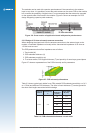
4.0 Manufacturing process recommendations
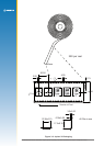
The Jupiter 32 uses the latest Land Grid Array (LGA) technology. Solder interconnect is
formed solely by solder paste applied to the board assembly. This results in a low stand-off
height, depending on solder paste volume and Printed Circuit Board (PCB) geometry. This
makes LGA ideal for small form-factor applications. Solder joint reliability studies indicate that
LGA greatly exceed typical industry reliability.
4.1 Solder methods
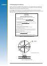
The Jupiter 32 has 34 surface mount connection pads that have a base metal of copper
with an Electroless Nickel Immersion Gold (ENIG) nish. This is suitable for a lead free
manufacturing process. Critical factors to ensure successful circuit board assembly with LGA
devices include, the design of the solder paste stencil, the solder paste and reow prole
used. Stencil attributes that have been shown to succeed in tests are solder stencil thickness,
aperture diameter, paste release characteristics, and practices to ensure consistent solder
paste volumes that exceed recommended minimums.
4.1.1 Solder paste type
The module will accept all commonly used solder pastes. The solder paste can be lead
based or lead-free. In all processes, factors such as circuit board thickness, fabrication
complexity, assembly process compatibility, and surface nish should be taken into
consideration. Also, due to the low standoff height of LGA devices and difculty cleaning, a
no-clean paste is recommended.
4.1.2 Solder paste mask size
Solder paste mask size should be adjusted by experimentation according to the production
process requirements. As a starting point, a 0.75:1 (paste mask:pad size) ratio is
recommended.
4.1.3 Solder paste stencils
A 0.125 mm (5 mil) thick stencil is recommended with LGA.
4.1.4 Reow prole recommendations
An optimal reow prole depends on solder paste properties and should be optimised and
proven out as part of an overall process development. The following guidelines represent
good soldering practices to help yield high quality assemblies with minimum rework.
It is important to provide a solder reow prole that matches the solder paste supplier’s
recommendations. Some uxes need a long dwell time below the temperature of 180°C,
while others will be burned up in a long dwell. Temperatures out of bounds of the solder paste
ux recommendation could result in poor solderability of components on the board. Solder
paste suppliers can recommend an suitable reow prole to give the best solderability. The
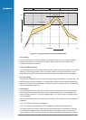
maximum reow temperature is 260 °C for 10 seconds.
The typical reow prole consists of four sections. In the preheat section, the PCB assembly
should be preheated at the maximum rate of 1° to 2° C/sec to start the solvent evaporation
and to avoid thermal shock. The assembly can then be heated for 60 to 120 seconds to
remove solder volatiles and activate the ux so the temperature of the package rises above
100° C. The reow section of the prole, the time above liquidus (approx. 185° C), can be
between 45 to 60 seconds with a peak temperature in the range of 230° to 260° C. This
allows all solder joints on the assembly to fully reow and a maximum peak temperature that
is below the maximum that the devices or solder material can tolerate. Finally, the assembly
can undergo cool-down in the fourth section of the liquidus point (approx. 185° C). The actual
prole parameters depends upon the recommendations of the solder paste supplier and
other reow requirements of the customer’s PCB.
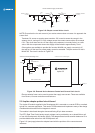
Refer to Figure 4-1 for sample lead and lead-free reow proles.