


LA000605D © 2007 Navman New Zealand. All rights reserved. Proprietary information and specications subject to change without notice.
7
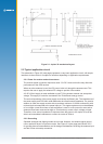
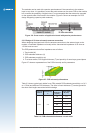
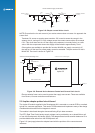
The modules can be used with a passive patch antenna if the connection to the antenna
input is very short. It is possible to mount the patch antenna on the same PCB as the module,
but to reduce the possibility of digital noise, it is recommended that the antenna be mounted
on the opposite side of the board to the module. (Figure 2-6 shows an example of a PCB
design integrating a passive patch antenna.)
Figure 2-6: Cross section of application board with passive patch antenna
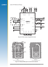
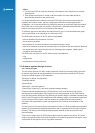
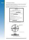
2.3.5 Design of 50 ohm microstrip antenna connection
When designing the signal track from the antenna connection to the antenna input on the
module, a controlled impedance microstrip with a characteristic impedance of 50 ohms at
1.5 GHz must be used.
The PCB parameters that affect impedance are as follows:
1. Track width (W)
2. PCB substrate thickness (H)
3. PCB substrate permittivity (ε
r
)
4. To a lesser extent, PCB copper thickness (T) and proximity of same layer ground plane.
Figure 2-7 shows a representation of the PCB microstrip and its parameters.
Figure 2-7: PCB microstrip dimensions
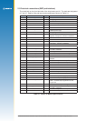
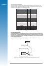
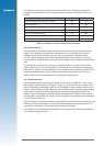
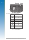
Table 2-3 shows typical track widths for an FR4 material PCB substrate (permittivity ε
r
of 4.3
at 1.5 GHz) and different PCB thickness. The effect of track thickness (T) can be ignored for
the short track lengths associated with this design.
Substrate
material
Permittivity
ε
r
Substrate
thickness
H (mm)
Track width
W (mm)
FR4 4.3
1.6 2.0
1.2 1.8
1.0 1.6
0.8 1.4
0.6 1.2
0.4 0.7
0.2 0.4
Table 2-3: PCB substrate thicknesses v track width