


LA000605D © 2007 Navman New Zealand. All rights reserved. Proprietary information and specications subject to change without notice.
5
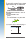
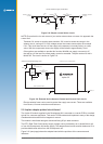
2.2.3 Decoupling
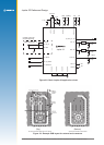
The schematic in Figure 2-2 illustrates a suggested method of decoupling that may be
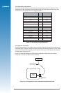
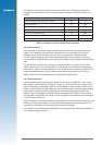
followed. Table 2-2 suggests decoupling values for all signals relative to the function required.
This level of decoupling may not be required in a particular application, in which case
these capacitors could be omitted. As shown in Figure 2-2, only the signal lines used in the
application require decoupling.
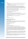
All capacitors are highly recommended if the module will experience substantial
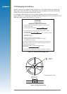
electromagnetic interference (EMI). All low value capacitors should be as close as possible to
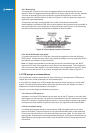
the module pad with a short connection to the ground plane (see Figure 2-4). Any data lines
that have not been properly shielded are susceptible to data corruption.
Figure 2-4: Decoupling Capacitor Placement
2.2.4 Serial RS232 data level shifter
To connect the module to a PC COM port, the serial data signals must be level shifted to
RS232 levels. This has not been shown in the reference design, but many single chip RS232
level shifters are available, such as MAX3232.
Note: It is highly recommended to provide test points on the serial data lines and ‘BOOT’
signal (pad C4), even if the application circuit does not use these signals. This will allow the
user to connect to these signals if a rmware upload or new conguration is required. These
test points can take the form of an untted ‘through-hole’ connector. Refer to Figure 2-2.
2.3 PCB design recommendations
The modules are surface mounted devices, hence the layout of the application PCB plays an
integral part in the overall performance of the nished system.
It is not difcult to design such a PCB, despite the presence of high frequency, low level radio
signals. The following recommendations have been offered to allow the designer to create a
design that will meet the requirements of this product.
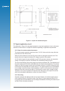
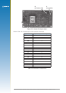
Figure 2-1 shows the copper pad dimensions and layout.
2.3.1 Choice of PCB stack up
In general, a two layer PCB substrate can be used, with all the RF signals on one side. Multi-
layer boards can also be used. The design recommendations here only address the microstrip
style of RF connection. Stripline designs can also be accommodated, however, long lengths
of stripline can cause excessive signal loss and vias in the signal track should be avoided.
2.3.2 Ground plane design
A complete ground plane should be used under the PCB with signal tracks on the same
layer as the module. The ground return for any signal should ideally have a clear path back
to its source and should not mix with other signal’s ground return paths. For this reason, RF
signal ground, underneath the microstrip antenna connection, should not be shared with any
digital signal or power supply return paths. Pads A2 and B1 are the RF signal ground return
connections.