


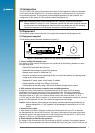
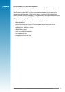
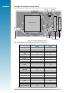
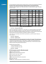
ON/OFF switch conguration DIP
switch
function LEDS JB5/6 reset switch
serial port 1
serial port 2
timing connector
DR connector
DC power
JB10/11/12
voltage selection
switch (3.3V or 5V)
JB1/2
JB3/4
JB13/14/15
test points E1 to E9
JB16/17
SW3
all off except SW3.3
9
LA000510C © 2006 Navman NZ Ltd. All rights reserved. Proprietary information and specications subject to change without notice.
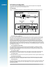
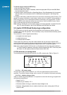
3.4 Clock out connector
The Clock out connector provides an interface for all associated timing signals with the module.
It provides the user access to the Time Mark (1PPS) signal. The pinout connections are
described in Table 3-2, and illustrated in Figure 3-4.
Pin number Function
1 not used
2 inverted 1PPS signal
3 normal 1PPS signal
4 ground
Table 3-2 Pin functions of the clock out connector
4
3
2
1
Figure 3-4 Pin layout of the clock out connector
A mating connector for the clock out connector is supplied with the Development kit. The part
number is shown in Table 3-3.
Manufacturer Part number
Molex 70400 series ‘G’
Table 3-3 Mating connector part description
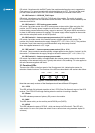
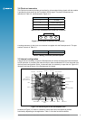
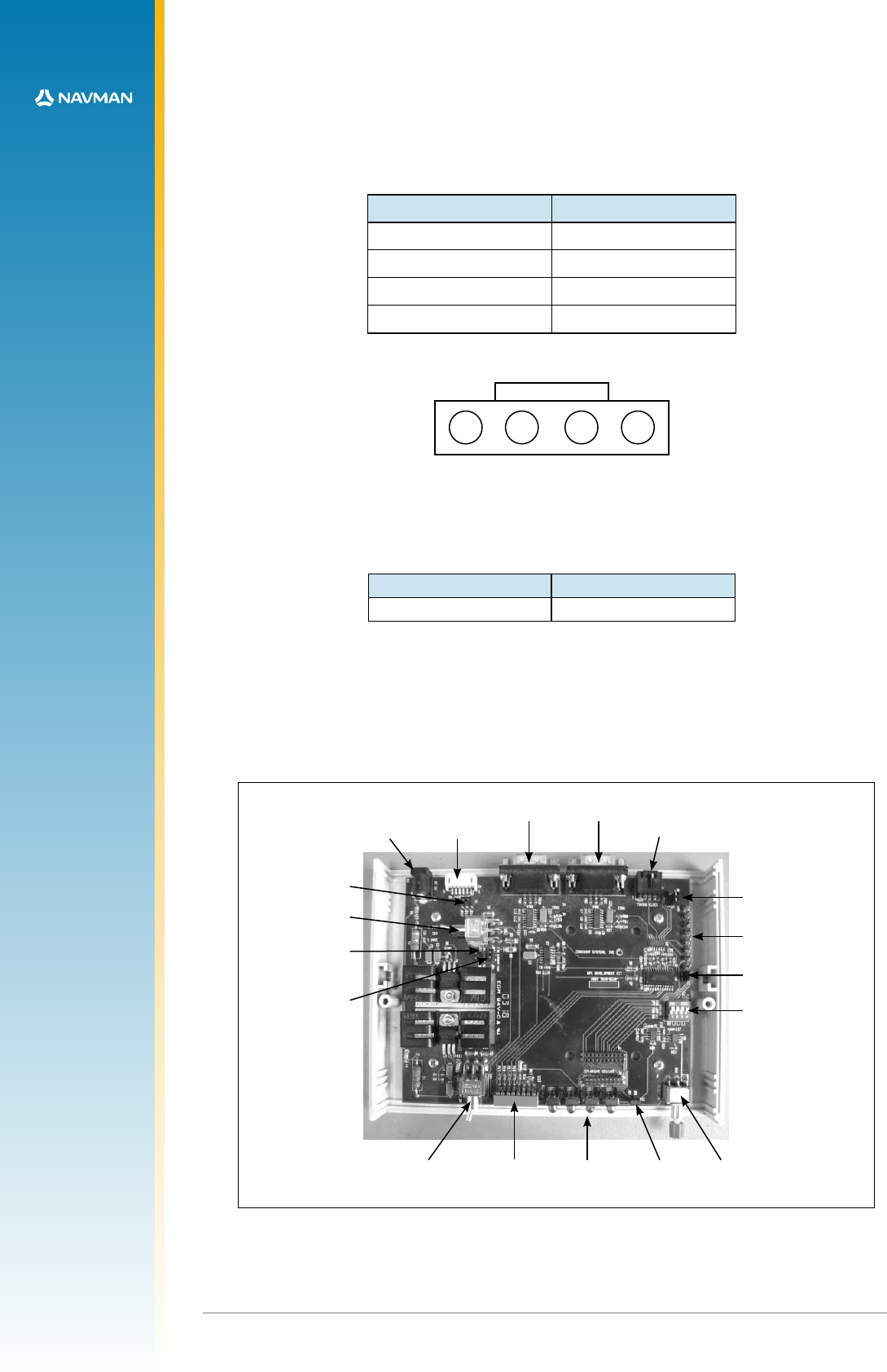
3.5 Internal conguration
It should not be necessary to open the Development Unit unless changing the internal switches
for DR operation or accessing the internal test pins. Most combinations of I/O can be made from
the front panel conguration switch. In the event that it is necessary to open the unit, Figure 3-5
illustrates the internal layout of the Development Unit board.
Figure 3-5 Internal layout of the Development Unit
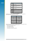
As shown in Figure 3-5, there is a selection of links that can be congured to provide
functionality depending on the application. Table 3-4 lists the functions available.