


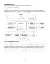
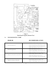

The block diagram in Figure 3 below shows the interaction between the various Main Board circuits.
Figure 3
Main Board Block Diagram
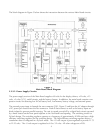
1.2.2.2 Power Supply Circuits
The power supply section of the Main Board supplies +60 volts for the display drivers, ±12 volts, +15
volts, +5 volts (VCC), on/off circuits, and the battery charger. In addition, the main board contains com-
parator circuits for detecting low NiCad battery level, low memory battery voltage, and external power.
The external power input is through the rear connector (J101, Figure 5) and from the AC adapter through
a DC power jack located near the rear connector. Both of these sources as well as the battery input are
diode isolated to prevent parallel sourcing. The unit is turned on and off by a digital latch circuit operated
by a knob located on the front panel adjacent to the NavData® card opening. The switching circuit is a
fly-back design. The switching regulator operates at a frequency of approximately 40 KHz and uses a high
efficiency switching regulator for the switching device. The high efficiency switching regulator drives a
transformer that is configured in a fly-back mode. The +15 volt output is post-regulated to provide 11.75
to 12.25 volts. The +5 volt output is regulated at 4.8 to 5.2 volts. All other voltages are ±20%.
4