


11
LA000578A © 2006 Navman New Zealand. All rights reserved. Proprietary information and specifications subject to change without notice.
4
3
2
1
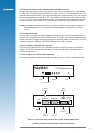
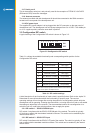
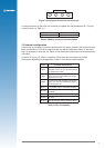
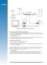
Figure 3-4 Pin layout of the clock out connector
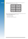
A mating connector for the clock out connector is supplied with the development kit. The part
number is shown in Table 3-3.
Manufacturer Part number
Molex 70400 series ‘G’
Table 3-3 Mating connector part description
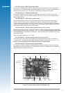
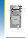
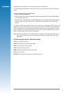
3.5 Internal conguration
It should not be necessary to open the development unit unless accessing the internal test pins.
Most combinations of I/O can be made from the front panel conguration switch. In the event
that it is necessary to open the unit, Figure 3-5 illustrates the internal layout of the development
unit board.
As shown in Figure 3-5, there is a selection of links that can be congured to provide
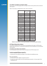
functionality depending on the application. Table 3-4 lists the functions available.
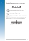
Pins Function when linked
JB1/2
Current link for 5 V supply. Can be used to
determine current on 5 V rail. Not used for
the Jupiter 30 module.
JB3/4
Current link for the primary power 3.3 V
supply. Can be used to determine supply
current for 3.3 V rail.
JB5/6
Current link for the secondary power RTC
supply. Can be used to determine supply
current for RTC rail.
JB10/11 5 V supplied to Pin 1 of the DR connector
JB11/12
3.3 V supplied to Pin 1 of the DR
connector
JB13/14 not used
JB14/15 not used
JB16/17 Internal interface enable (normally tted)
Table 3-4 Pin functionality