


SSM2166
REV. A
–8–
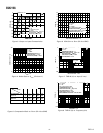
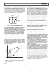
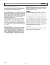
10
0%
100
90
100mV
1S
6dBV
66dBV
85dBV
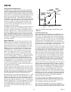
Figure 15b. RMS Level Detector Performance with
C
AVG
= 22
µ
F
Control Circuitry
The output of the rms level detector is a signal proportional to
the log of the true rms value of the buffer output with an added
dc offset. The control circuitry subtracts a dc voltage from this
signal, scales it, and sends the result to the VCA to control the
gain. The VCA’s gain control is logarithmic—a linear change in
control signal causes a dB change in gain. It is this control law
that allows linear processing of the log rms signal to provide the
flat compression characteristic on the input/output characteristic
shown in Figure 13.
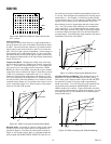
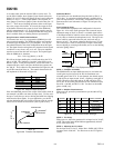
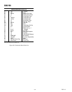
Compression Ratio. Changing the scaling of the control sig-
nal fed to the VCA causes a change in the circuit’s compression
ratio, “r.” This effect is shown in Figure 16. The compression
ratio can be set by connecting a resistor between the COMP
RATIO pin (Pin 10) and GND. Lowering R
COMP
gives smaller
compression ratios as indicated in Figure 5, with values of about
17 kΩ or less resulting in a compression ratio of 1:1. AGC per-
formance is achieved with compression ratios between 2:1 and
15:1, and is dependent on the application. A 100 kΩ potentiom-
eter may be used to allow this parameter to be adjusted. On the
evaluation board (Figure 22), an optional resistor can be used to
set the compression equal to 1:1 when the wiper of the potenti-
ometer is at its full CCW position.
INPUT – dB
OUTPUT – dB
V
DE
V
RP
15:1
5:1
2:1
1:1
1
1
VCA GAIN
Figure 16. Effect of Varying the Compression Ratio
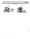
Rotation Point. An internal dc reference voltage in the control
circuitry, used to set the rotation point, is user-specified, as il-
lustrated in Figure 9. The effect on rotation point is shown in
Figure 17. By varying a resistor, R
ROT PT
, connected between the
positive supply and the ROTATION POINT SET pin (Pin 11),
the rotation point may be varied from approximately 20 mV rms
to 1 V rms. From the figure, the rotation point is inversely propor-
tional to R
ROT PT
. For example, a 1 kΩ resistor would typically
set the rotation point at 1 V rms, whereas a 55 kΩ resistor would
typically set the rotation point at approximately 30 mV rms.
Since limiting occurs for signals larger than the rotation point
(V
IN
> V
RP
), the rotation point effectively sets the maximum
output signal level. It is recommended that the rotation point
be set at the upper extreme of the range of typical input signals
so that the compression region will cover the entire desired in-
put signal range. Occasional larger signal transients will then be
attenuated by the action of the limiter.
V
DE
V
RP1
INPUT – dB
OUTPUT – dB
V
RP2
V
RP3
VCA GAIN
1
1
r:1
Figure 17. Effect of Varying the Rotation Point
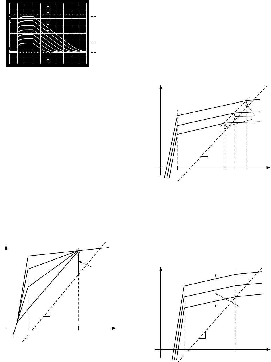
VCA Gain Setting and Muting. The maximum gain of the
SSM2166 is set by the GAIN ADJUST pin (Pin 2) via R
GAIN
.
This resistor, with a range between 1 kΩ and 20 kΩ, will cause
the nominal VCA gain to vary from 0 dB to approximately
20 dB, respectively. To set the VCA gain to its maximum can
also be achieved by leaving the GAIN ADJUST pin in an
OPEN condition (no connect). Figure 18 illustrates the effect
on the transfer characteristic by varying this parameter. For low
level signal sources, the VCA should be set to maximum gain
using a 20 kΩ resistor.
INPUT – dB
OUTPUT – dB
V
DE
V
RP
VCA GAIN
1
1
r:1
Figure 18. Effect of Varying the VCA Gain Setting