


SSM2166
REV. A
–6–
APPLICATIONS INFORMATION
The SSM2166 is a complete microphone signal conditioning
system on a single integrated circuit. Designed primarily for
voiceband applications, this integrated circuit provides amplifi-
cation, rms detection, limiting, variable compression, and down-
ward expansion. An integral voltage-controlled amplifier (VCA)
provides up to 60 dB of gain in the signal path with approxi-
mately 30 kHz bandwidth. Additional gain is provided by an
input buffer op amp circuit that can be set anywhere from 0 dB
to 20 dB, for a total signal path gain of up to 80 dB. The device
operates on a single +5 V supply, accepts input signals up to
1 V rms, and produces output signal levels > 1 V rms (3 V p-p)
into loads > 5 kΩ. The internal rms detector has a time con-
stant set by an external capacitor.
The SSM2166 contains an input buffer and automatic gain con-
trol (AGC) circuit for audio- and voiceband signals. Circuit
operation is optimized by providing a user-adjustable time con-
stant and compression ratio. A downward expansion (noise gat-
ing) feature eliminates circuit noise in the absence of an input
signal. The SSM2166 allows the user to set the downward ex-
pansion threshold, the limiting threshold (rotation point), input
buffer fixed gain, and the internal VCA’s nominal gain at the ro-
tation point. The SSM2166 also features a power-down mode
and muting capability.
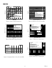
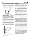
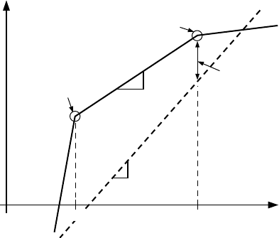
Theory of Operation
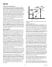
Figure 13 illustrates a typical transfer characteristic for the
SSM2166 where the output level in dB is plotted as a func-
tion of the input level in dB. The dotted line indicates the
transfer characteristic for a unity-gain amplifier. For input
signals in the range of V
DE
(Downward Expansion) to V
RP
(Rotation Point) an “r” dB change in the input level causes a
1 dB change in the output level. Here, “r” is defined as the
“compression ratio.” The compression ratio may be varied
from 1:1 (no compression) to over 15:1 via a single resistor,
R
COMP
. Input signals above V
RP
are compressed with a fixed
compression ratio of approximately 15:1. This region of opera-
tion is the “limiting region.” Varying the compression ratio has
no effect on the limiting region. The breakpoint between the
compression region and the limiting region is referred to as the
“limiting threshold” or the “rotation point,” and is user-specified
in the SSM2166. The term “rotation point” derives from the
observation that the straight line in the compression region
“rotates” about this point on the input/output characteristic as
the compression ratio is changed.
The gain of the system with an input signal level of V
RP
is fixed
by R
GAIN
regardless of the compression ratio, and is the “nomi-
nal gain” of the system. The nominal gain of the system may be
increased by the user via the onboard VCA by up to 20 dB. Ad-
ditionally, the input buffer of the SSM2166 can be configured
to provide fixed gains of 0 dB to 20 dB with R1 and R2.
Input signals below V
DE
are downward expanded; that is, a –1 dB
change in the input signal level causes approximately a –3 dB
change in the output level. As a result, the gain of the system is
small for very small input signal levels, even though it may be
quite large for small input signals above of V
DE
. The downward
expansion threshold, V
DE
, is set externally by the user via R
GATE
at Pin 9 (NOISE GATE). Finally, the SSM2166 provides an
active HIGH, CMOS-compatible digital input whereby a
power-down feature will reduce device supply current to less
than 100 µA.
INPUT – dB
OUTPUT – dB
LIMITING
REGION
LIMITING
THRESHOLD
(ROTATION POINT)
COMPRESSION
REGION
1
r
1
1
DOWNWARD
EXPANSION
THRESHOLD
(NOISE GATE)
DOWNWARD
EXPANSION
REGION
V
DE
V
RP
VCA GAIN
Figure 13. General Input/Output Characteristics of the
SSM2166
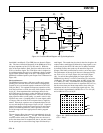
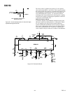
The SSM2166 Signal Path
Figure 14 illustrates the block diagram of the SSM2166. The
audio input signal is processed by the input buffer and then
by the VCA. The input buffer presents an input impedance
of approximately 180 kΩ to the source. A dc voltage of approxi-
mately 1.5 V is present at AUDIO +IN (Pin 7 of the SSM2166),
requiring the use of a blocking capacitor (C1) for ground-
referenced sources. A 0.1 µF capacitor is a good choice for most
audio applications. The input buffer is a unity-gain stable ampli-
fier that can drive the low impedance input of the VCA.
The VCA is a low distortion, variable-gain amplifier whose gain
is set by the side-chain control circuitry. The input to the VCA
is a virtual ground in series with approximately 1 kΩ. An exter-
nal blocking capacitor (C6) must be used between the buffer’s
output and the VCA input. The 1 kΩ impedance between am-
plifiers determines the value of this capacitor which is typically
between 4.7 µF and 10 µF. An aluminum electrolytic capacitor
is an economical choice. The VCA amplifies the input signal
current flowing through C6 and converts this current to a volt-
age at the SSM2166’s output pin (Pin 13). The net gain from
input to output can be as high as 60 dB (without additional
buffer gain), depending on the gain set by the control circuitry.
The gain of the VCA at the rotation point is set by the value of a
resistor connected between Pin 2 and GND, R
GAIN
. The rela-
tionship between the VCA gain and R
GAIN
is shown in Figure 6.
The AGC range of the SSM2166 can be as high as 60 dB. The
VCA
IN
pin (Pin 3) on the SSM2166 is the noninverting input
terminal to the VCA. The inverting input of the VCA is also
available on the SSM2166’s Pin 4 (VCA
R
) and exhibits an input
impedance of 1 kΩ, as well. As a result, this pin can be used for
differential inputs or for the elimination of grounding problems
by connecting a capacitor whose value equals that used in series
with the VCA
IN
pin, to ground. See Figure 22, SSM2166
Evaluation Board for more details.
The output impedance of the SSM2166 is typically less that
75 Ω, and the external load on Pin 13 should be >5 kΩ. The
nominal output dc voltage of the device is approximately 2.2 V.
Use a blocking capacitor for grounded loads.
The bandwidth of the SSM2166 is quite wide at all gain set-
tings. The upper 3 dB point is approximately 30 kHz at gains as
high as 60 dB (using the input buffer for additional gain, circuit