


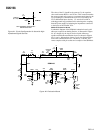

SSM2166
REV. A
–7–
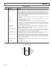
AUDIO
+IN
BUF
OUT
53
2
V
OUT
9
NOISE
GATE
11
ROTATION
POINT
ADJUST
10
1
GND
13
VCA
R
7
RMS
LEVEL
DETECTOR
INPUT
BUFFER
VCA
VCA
IN
SSM2166
R2 = 10k⍀
1F
CONTROL
CIRCUITRY
12
POWER
DOWN
POWER
DOWN
R
GAIN
COMPRESSION
RATIO SET
R
COMP
8
C
AVG
2.2F
AVG
CAP
GAIN
ADJUST
OUTPUT
1k⍀
4
1k⍀
C6
10F
V+
V+
R
GATE
R
ROT PT
GND
C7*
10F
*OPTIONAL
0.1F
R1 = 10k⍀
+
14
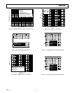
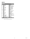
Figure 14. Functional Block Diagram and Typical Application
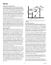
bandwidth is unaffected). The GBW plots are shown in Figure
10b. The lower 3 dB cutoff frequency of the SSM2166 is set by
the input impedance of the VCA (1 kΩ) and C6. While the
noise of the input buffer is fixed, the input referred noise of the
VCA is a function of gain. The VCA input noise is designed to
be a minimum when the gain is at a maximum, thereby optimiz-
ing the usable dynamic range of the part. A photograph of the
SSM2166’s wideband peak-to-peak output noise is illustrated in
Figure 10b.
The Level Detector
The SSM2166 incorporates a full-wave rectifier and a patent-
pending, true rms level detector circuit whose averaging time
constant is set by an external capacitor connected to the AVG
CAP pin (Pin 8). For optimal low frequency operation of the
level detector down to 10 Hz, the value of the capacitor should
be 2.2 µF. Some experimentation with larger values for the
AVG CAP may be necessary to reduce the effects of excessive
low frequency ambient background noise. The value of the aver-
aging capacitor affects sound quality: too small a value for this
capacitor may cause a “pumping effect” for some signals, while
too large a value can result in slow response times to signal dy-
namics. Electrolytic capacitors are recommended here for low-
est cost and should be in the range of 2 µF to 47 µF. Capacitor
values from 18 µF to 22 µF have been found to be more appro-
priate in voiceband applications, where capacitors on the low
end of the range seem more appropriate for music program
material.
The rms detector filter time constant is approximately given by
10•C
AVG
milliseconds where C
AVG
is in µF. This time constant
controls both the steady-state averaging in the rms detector as
well as the release time for compression; that is, the time it takes
for the system gain to react when a large input is followed by a
small signal. The attack time, the time it takes for the gain to be
reduced when a small signal is followed by a large signal, is con-
trolled partly by the AVG CAP value, but is mainly controlled
by internal circuitry that speeds up the attack for large level
changes. This limits overload time to under 1 ms in most cases.
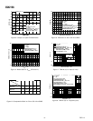
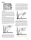
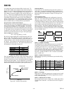
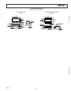
The performance of the rms level detector is illustrated in Fig-
ure 15 for a C
AVG
of 2.2 µF (Figure 15a) and 22 µF (Figure
15b). In each of these photographs, the input signal to the
SSM2166 (not shown) is a series of tone bursts in 6 successive
10 dB steps. The tone bursts range from –66 dBV (0.5 mV rms)
to –6 dBV (0.5 V rms). As illustrated in the photographs, the
attack time of the rms level detector is dependent only on C
AVG
,
but the release times are linear ramps whose decay times are
dependent on both C
AVG
and the input signal step size. The
rate of release is approximately 240 dB/s for a C
AVG
of 2.2 µF,
and 12 dB/s for a C
AVG
of 22 µF.
10
0%
100
90
100mV
100ms
6dBV
66dBV
85dBV
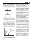
Figure 15a. RMS Level Detector Performance with
C
AVG
= 2.2
µ
F