


SSM2166
REV. A
–10–
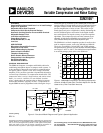
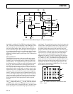
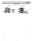
C
X
1000pF
C1
0.1F
AUDIO IN
(R
S
> 5k⍀)
7
+IN
SSM2166
NOTE: ADDITIONAL CIRCUIT DETAILS
OMITTED FOR CLARITY.
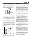
Figure 21. Circuit Configuration for Use with High
Impedance Signal Sources
The value of the C7 should be the same as C6, the capacitor
value used between BUF
OUT
and VCA
IN
. This connection makes
the source ground noise appear as a common-mode signal to the
VCA, allowing the common-mode noise to be rejected by the
VCA’s differential input circuitry. C7 can also be useful in
reducing ground loop problems and in reducing noise coupling
from the power supply by balancing the impedances connected
to the inputs of the internal VCA.
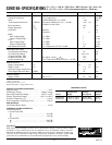
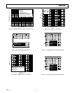
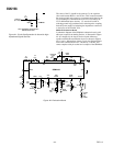
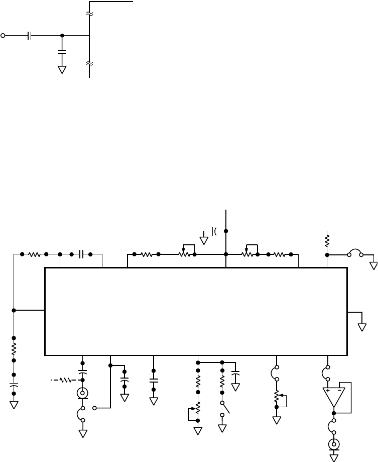
SSM2166 Evaluation Board
A schematic diagram of the SSM2166 evaluation board, avail-
able upon request from Analog Devices, is illustrated in Figure
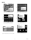
22. As a design aid, the layouts for the topside silkscreen,
topside and backside metallization layers are shown in Figures
23a, b, and c. Although not shown to scale, the finished dimen-
sion of the evaluation board is 3.5 inches by 3.5 inches, and
comes complete with pin sockets and a sample of the SSM2166.
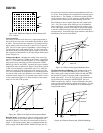
Figure 22. Evaluation Board
ROT PT.
ADJ
NOISE
GATE
ADJ
9
R7
1M⍀
CW
R8
1k⍀
C3
0.1F
+V
R12
100k⍀
J3
NOISE
GATE
POWER
DN
V+
14
BUF
OUT
VCA
IN
C6
10F
+
53
VCA
R
7
+INPUT
MIC
PWR
INPUT
JACK
1/8"
PHONE
C1
0.1F
3
1
2
C7
10F
+
4
GAIN
ADJUST
MUTE
SWITCH
R11
330⍀
2
R9
1k⍀
CW
R10
20k⍀
C5
0.01F
GAIN
ADJ
AVG
CAP
+
8
C4
22F
1
–INPUT
SSM2166
6
R2
10k⍀
C2
1F
COMP
RATIO
10
CW
R6
100k⍀
COMP
RATIO
13
5
4
OP113
6
7
OUTPUT
JACK
RCA
PHONO
OUTPUT
CW
R3
50k⍀
R4
1k⍀
ROTATION
PT ADJ
11
R1
10k⍀
12
GND