


SSM2166
REV. A
–9–
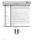
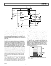
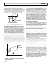
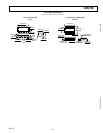
The gain of the VCA can be reduced below 0 dB by making
R
GAIN
smaller than 1 kΩ. Switching Pin 2 through 330 Ω or less
to ground will mute the output. Either a switch connected to
ground or a transistor may be used, as shown in Figure 19. To
avoid audible “clicks” when using this MUTE feature, a capaci-
tor (C5 in figure) can be connected from pin 2 to GND. The
value of the capacitor is arbitrary and should be determined em-
pirically, but a 0.01 µF capacitor is a good starting value.
GAIN
ADJUST
C5
R
GAIN
330⍀
MUTE
(CLOSED SWITCH)
NOTE: ADDITIONAL CIRCUIT DETAILS
OMITTED FOR CLARITY.
SSM2166
2
Figure 19. Details of SSM2166 Mute Option
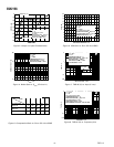
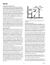
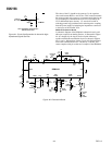
Downward Expansion Threshold. The downward expan-
sion, or noise gate, threshold is determined via a second refer-
ence voltage internal to the control circuitry. This second
reference can be varied in the SSM2166 using a resistor, R
GATE
,
connected between the positive supply and the NOISE GATE
SET pin (Pin 9) of the SSM2166. The effect of varying this
threshold is shown in Figure 20. The downward expansion
threshold may be set between 300 µV rms and 20 mV rms by
varying the resistance value between Pin 9 and the supply volt-
age. Like the ROTATION PT ADJUST, the downward expan-
sion threshold is inversely proportional to the value of this
resistance: setting this resistance to 1 MΩ sets the threshold at
approximately 250 µV rms, whereas a 10 kΩ resistance sets the
threshold at approximately 20 mV rms. This relationship is
illustrated in Figure 4. A potentiometer network is provided on
the evaluation board for this adjustment. In general, the down-
ward expansion threshold should be set at the lower extreme of
the desired range of the input signals, so that signals below this
level will be attenuated.
VCA GAIN
INPUT – dB
OUTPUT – dB
V
DE1
V
RP
V
DE3
V
DE2
1
1
r:1
Figure 20. Effect of Varying the Downward Expansion
(Noise Gate) Threshold
Power-Down Feature
The supply current of the SSM2166 can reduced to under
100 µA by applying an active HIGH, 5 V CMOS compatible
input to the SSM2166’s POWER DOWN pin (Pin 12). In this
state, the input and output circuitry of the SSM2166 will assume a
high impedance state; as such, the potentials at the input pin
and the output pin will be determined by the external circuitry
connected to the SSM2166. The SSM2166 takes approximately
200 ms to settle from a POWER-DOWN to POWER-ON com-
mand. For POWER-ON to POWER-DOWN, the SSM2166
requires more time, typically less than 1 s. Cycling the power
supply to the SSM2166 can result in quicker settling times: the
off-to-on settling time of the SSM2166 is less than 200 ms,
while the on-to-off settling time is less than 1 ms. In either
implementation, transients may appear at the output of the de-
vice. In order to avoid these output transients, MUTE control
of the VCA’s gain as previously mentioned should be used.
PC Board Layout Considerations
Since the SSM2166 is capable of wide bandwidth operation and
can be configured for as much as 80 dB of gain, special care
must be exercised in the layout of the PC board which contains
the IC and its associated components. The following applica-
tions hints should be considered and/or followed:
(1) In some high system gain applications, the shielding of in-
put wires to minimize possible feedback from the output of the
SSM2166 back to the input circuit may be necessary.
(2) A single-point (“star”) ground implementation is recom-
mended in addition to maintaining short lead lengths and PC
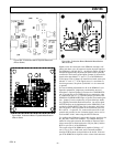
board runs. The evaluation board layout shown in Figure 23 for
the SSM2166 demonstrates the single-point grounding scheme.
In applications where an analog ground and a digital ground are
available, the SSM2166 and its surrounding circuitry should be
connected to the system’s analog ground. As a result of these
recommendations, wire-wrap board connections and grounding
implementations are to be explicitly avoided.
(3) The internal buffer of the SSM2166 was designed to drive
only the input of the internal VCA and its own feedback net-
work. Stray capacitive loading to ground from the BUF
OUT
pin
in excess of 5 pF to 10 pF can cause excessive phase shift and
can lead to circuit instability.
(4) When using high impedance sources (≥ 5 kΩ), system gains
in excess of 60 dB are not recommended. This configuration is
rarely appropriate, as virtually all high impedance inputs provide
larger amplitude signals that do not require as much amplifica-
tion. When using high impedance sources, however, it can be
advantageous to shunt the source with a capacitor to ground at
the input pin of the IC (Pin 7) to lower the source impedance at
high frequencies, as shown in Figure 21. A capacitor with a value
of 1000 pF is a good starting value and sets a low pass corner at
31 kHz for 5 kΩ sources. In those applications where the source
ground is not as “clean” as would be desirable, a capacitor (illus-
trated as C7 on the evaluation board) from the VCA
R
input to
the source ground might prove beneficial. This capacitor is
used in addition to the grounded capacitor (illustrated as C2 on
the evaluation board) used in the feedback around the buffer,
assuming that the buffer is configured for gain.