


27.1.1999
4Z0700GB.__2
36
Product: TDP-52-SN3 (Sigma Gold) / Synthesizer
5.3 RF MODULE
RX Synthesizer
Synthesizer
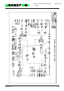
5.3.1 General
The RX synthesizer generates an upper side injection frequency for the receiver.
The injection frequency is fed to the receiver’s first mixer.
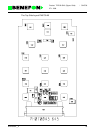
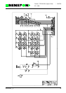
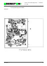
5.3.2 Functional Description
The RX injection frequency is generated with a phase locked loop. The VCO pro-
duces the injection frequency determined by the control voltage. After the VCO
stage comes the amplifier stage Q320. After the amplifier stage, part of the signal is
fed to the synthesizer circuits I300 divider. The synthesizer circuit contains a pre-
scaler, programmable divider, reference frequency divider, and a phase detector.
The synthesizer circuit produces current pulses at output DO1 as controlled by the
phase detector. The current pulses either charge or discharge the loop filter. The
VCO control voltage is derived from the loop filter output.
The synthesizer 12.5 kHz reference frequency is made by dividing the 12.8 MHz sig-
nal from the temperature compensated oscillator (TCXO). The series-form signal
which controls the channel frequency comes from the audio/processor-module via
connector V600. SDATA, SCLK and SLE signals are common to both TX- and RX-
synthesizers. A positive pulse in the SLE line loads the division ratio (corresponding
to the frequency of the channel) fed to the SDATA line, to the synthesizer circuit
I300.
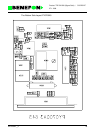
5.3.3 Control- and Output-Signals
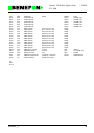
Operating voltage 4.75VDC
Current consumption 14 mA
Output level to the receiver +1 dBm
Frequency range 540,25...544,725 MHz
VRX RX synthesizer operating voltage 4.75V
SCLK Clock signal for the synthesizer control data
SDATA Synthesizer control data
SLE ENABLE pulse to the synthesizer
RXINJ RX synthesizer output to the receiver +1 dBm
RX_REG Control line for VRX-regulator