


27.1.1999
8dds50gb_fm5.fm
7
Product: DDS-50(Office set) / YO0311
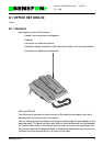
8.1.3 Operation
8.1.3.1 General
Power supply unit is connected to one of the connectors on the back of the unit.
Connections on these two connectors are identical to each other. Supply voltage
(VB) turns on regulator I124 which is used to generate +5 VDC supply (VCC) for pro-
cessor and other electronics. Note that the power amplifiers of the earphone signal,
I499 and I528 do not use VCC but VB instead. Once the VCC signal has risen, also
signal CADET is activated. This causes the phone to communicate with the I2C cir-
cuit and register that office kit is present.
8.1.3.2 Processor / charging
The processor I264 is National Semiconductor COPCF888. Crystal frequency used
is 8,00 MHz.
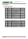
I/O pins/signals are as follows:
A/D input I3 is used to measure the voltage of the spare battery. Amplifier I277 con-
verts the input voltage level into the new range which is suitable for A/D input. Out-
put G3 is a PWM signal which is converted with R291 and C293 into analog DC
signal. This signal is used to control the output current of the power supply unit. Out-
puts D0 and D1 are used to turn on charging current for the phone and spare bat-
tery. P-channel fets Q211 and Q221 are normally in non-conducting state (gate
voltage tied to VB) and are turned on with fets Q212 and Q222 as the control signal
has been activated. In normal operation fets Q211 and Q221 are never simulta-
neously in the conducting state.
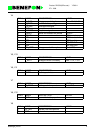
I/O SIGNALS DIRECTION
C0 spare battery discharge switch IN
C7 battery pack memory IN / OUT
D0 phone charge fet control OUT
D1 spare battery charge fet control OUT
D2 spare battery discharge control OUT
D3 phone detect current control OUT
D4 phone charge indicator (red) controlOUT
D5 phone charge indicator (green) control OUT
D6 spare battery charge indicator (red) control OUT
D7 spare battery charge indicator (green) control OUT
G3 power supply control OUT
I0 charger control from phone IN
I1 spare battery temperature IN
I2 phone battery voltage IN
I3 spare battery voltage IN
I4 PWM_CHK (not used) IN