


27.1.1999
4A0701GB.__1
5
Product: TDP-52-SN3 (Sigma Gold) / OA0701 Processor
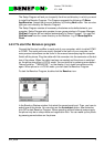
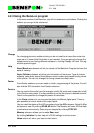
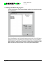
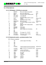
5.1.2.3 Display Module, A101
5.1.2.4 Answer Module, I101
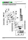
5.1.3 Circuit Diagram
The processor and audio circuit diagram is split into five parts. Signals in the
circuit diagrams have been given names, and signals with the same name are
connected between diagrams.
1 VCC supply voltage 5V
2 RES reset-line 0/5V
3 CSI display data input 0/5V
4AO
5 SCL clock line for data 0/5V
6SI
7 GND ground
8 CONT not function
9GND
10 LED supply voltage for led of display
11 KEYOUT1 key matrix output (volume key -) 0/5V
12 KEYINP4
13 KEYINP4 key matrix input (volume keys+/-) 0/5V
14 KEYOUT0 key matrix output (volume key +) 0/5V
15 PWRKEY powerkey
16 GND
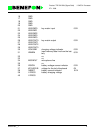
1 VCC supply voltage 5V
2 REC record control 0/5V
3 GND ground
4PLAYE 5V
5 PLAYL play control 0/5V
6 ANAIN audio input
7 GND1 ground
8 VCCA supply voltage 5V
9 SP+ audio output
10 GND2 ground