


R3111x
14
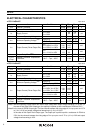
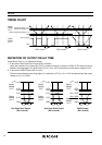
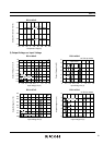
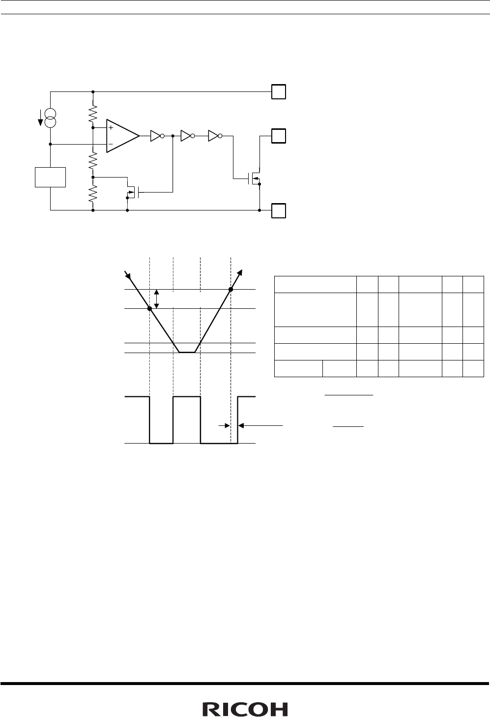
OPERATION
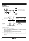
• Operation of R3111xxxxA
Vref
Ra
Rb
Rc
V
DD
OUT
GND
Tr.1
Nch
Com
p
arato
r
OUT pin should be pulled-up to
V
DD
or an external voltage level.
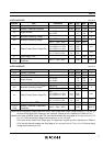
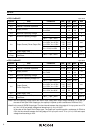
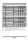
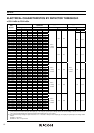
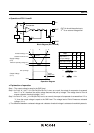
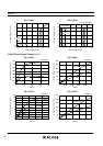
Block Diagram (R3111xxxxA)
13 5
A
B
t
PLH
2 4
GND
GND
V
DDL
-
V
DET
+V
DET
Detector Threshold
Released Voltage
Minimum Operating Voltage
Pull-up Voltage
Detector Threshold
Hysteresis
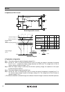
Supply Voltage
(V
DD
)
Output Voltage
(V
OUT
)
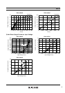
Step 1 2 3 4 5
Comparator (+)
Pin Input Voltage
I II II II I
Comparator Output H L Indefinite L H
Tr.1 OFF ON Indefinite ON OFF
Output Tr. Nch OFF ON Indefinite ON OFF
I
×V
DD
Rb+Rc
Ra+Rb+Rc
II
×V
DD
Rb
Ra+Rb
Operation Diagram
• Explanation of operation
Step 1. The output voltage is equal to the pull-up voltage.
Step 2. At Point “A”, Vref
>
=
VDD×(Rb+Rc)/(Ra+Rb+Rc) is true, as a result, the output of comparator is reversed
from "H" to "L", therefore the output voltage becomes the GND level. The voltage level of Point A means
a detector threshold voltage (−V
DET).
Step 3. When the supply voltage is lower than the minimum operating voltage, the operation of the output
transistor becomes indefinite. The output voltage is equal to the pull-up voltage.
Step 4. The output Voltage is equal to the GND level.
Step 5. At Point “B”, Vref
<
=
VDD×Rb/(Ra+Rb) is true, as a result, the output of comparator is reversed from "L" to
"H", then the output voltage is equal to the pull-up voltage. The voltage level of Point B means a released
voltage (+V
DET).
∗) The difference between a released voltage and a detector threshold voltage is a detector threshold hysteresis.
Output
Delay Time