


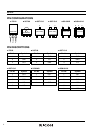
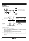
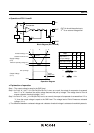
R3111x
12
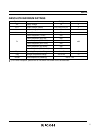
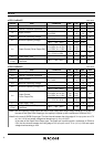
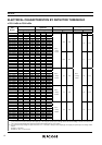
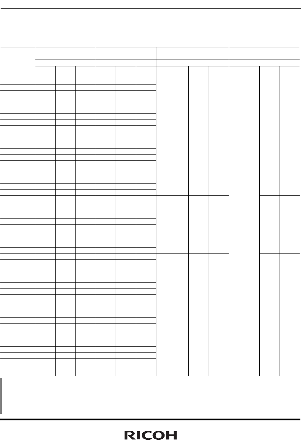
ELECTRICAL CHARACTERISTICS BY DETECTOR THRESHOLD
• R3111x09x to R3111x60x
Detector Threshold
Detector Threshold
Hysteresis
Supply Current 1 Supply Current 2
−VDET
[
V
]
V
HYS
[
V
]
I
SS1
[
µA
]
I
SS2
[
µA
]
Part
Number
Min. Typ. Max. Min. Typ. Max. Condition Typ. Max. Condition Typ. Max.
R3111x09xx 0.882 0.900 0.918 0.027 0.045 0.063 0.9 2.7
R3111x10xx 0.980 1.000 1.020 0.030 0.050 0.070
R3111x11xx 1.078 1.100 1.122 0.033 0.055 0.077
R3111x12xx 1.176 1.200 1.224 0.036 0.060 0.084
R3111x13xx 1.274 1.300 1.326 0.039 0.065 0.091
R3111x14xx 1.372 1.400 1.428 0.042 0.070 0.098
R3111x15xx 1.470 1.500 1.530 0.045 0.075 0.105
R3111x16xx 1.568 1.600 1.632 0.048 0.080 0.112
R3111x17xx 1.666 1.700 1.734 0.051 0.085 0.119
R3111x18xx 1.764 1.800 1.836 0.054 0.090 0.126
R3111x19xx 1.862 1.900 1.938 0.057 0.095 0.133
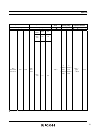
0.8 2.4
1.0 3.0
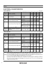
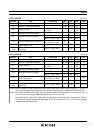
R3111x20xx 1.960 2.000 2.040 0.060 0.100 0.140
R3111x21xx 2.058 2.100 2.142 0.063 0.105 0.147
R3111x22xx 2.156 2.200 2.244 0.066 0.110 0.154
R3111x23xx 2.254 2.300 2.346 0.069 0.115 0.161
R3111x24xx 2.352 2.400 2.448 0.072 0.120 0.168
R3111x25xx 2.450 2.500 2.550 0.075 0.125 0.175
R3111x26xx 2.548 2.600 2.652 0.078 0.130 0.182
R3111x27xx 2.646 2.700 2.754 0.081 0.135 0.189
R3111x28xx 2.744 2.800 2.856 0.084 0.140 0.196
R3111x29xx 2.842 2.900 2.958 0.087 0.145 0.203
V
DD=
(
−VDET)
−0.10V
0.9 2.7 1.1 3.3
R3111x30xx 2.940 3.000 3.060 0.090 0.150 0.210
R3111x31xx 3.038 3.100 3.162 0.093 0.155 0.217
R3111x32xx 3.136 3.200 3.264 0.096 0.160 0.224
R3111x33xx 3.234 3.300 3.366 0.099 0.165 0.231
R3111x34xx 3.332 3.400 3.468 0.102 0.170 0.238
R3111x35xx 3.430 3.500 3.570 0.105 0.175 0.245
R3111x36xx 3.528 3.600 3.672 0.108 0.180 0.252
R3111x37xx 3.626 3.700 3.774 0.111 0.185 0.259
R3111x38xx 3.724 3.800 3.876 0.114 0.190 0.266
R3111x39xx 3.822 3.900 3.978 0.117 0.195 0.273
V
DD=
(
−VDET)
−0.13V
1.0 3.0 1.2 3.6
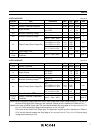
R3111x40xx 3.920 4.000 4.080 0.120 0.200 0.280
R3111x41xx 4.018 4.100 4.182 0.123 0.205 0.287
R3111x42xx 4.116 4.200 4.284 0.126 0.210 0.294
R3111x43xx 4.214 4.300 4.386 0.129 0.215 0.301
R3111x44xx 4.312 4.400 4.488 0.132 0.220 0.308
R3111x45xx 4.410 4.500 4.590 0.135 0.225 0.315
R3111x46xx 4.508 4.600 4.692 0.138 0.230 0.322
R3111x47xx 4.606 4.700 4.794 0.141 0.235 0.329
R3111x48xx 4.704 4.800 4.896 0.144 0.240 0.336
R3111x49xx 4.802 4.900 4.998 0.147 0.245 0.343
V
DD=
(
−VDET)
−0.16V
1.1 3.3 1.3 3.9
R3111x50xx 4.900 5.000 5.100 0.150 0.250 0.350
R3111x51xx 4.998 5.100 5.202 0.153 0.255 0.357
R3111x52xx 5.096 5.200 5.304 0.156 0.260 0.364
R3111x53xx 5.194 5.300 5.406 0.159 0.265 0.371
R3111x54xx 5.292 5.400 5.508 0.162 0.270 0.378
R3111x55xx 5.390 5.500 5.610 0.165 0.275 0.385
R3111x56xx 5.488 5.600 5.712 0.168 0.280 0.392
R3111x57xx 5.586 5.700 5.814 0.171 0.285 0.399
R3111x58xx 5.684 5.800 5.916 0.174 0.290 0.406
R3111x59xx 5.782 5.900 6.018 0.177 0.295 0.413
R3111x60xx 5.880 6.000 6.120 0.180 0.300 0.420
V
DD=
(
−VDET)
−0.20V
1.2 3.6
V
DD=
(
−VDET)
+2.0V
1.4 4.2
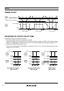
*1)
In the case of CMOS output type; when the voltage is forced to V
DD
from 0.7V to (
+
V
DET
)
+
2.0V, time interval between the rising edge of V
DD
and the reaching point at
((
+
V
DET
)
+
2.0V)/2. In the case of Nch open drain output type : The output pin is pulled up to 5V through 470k
Ω
, and when the voltage is forced to V
DD
from 0.7V to
(
+
V
DET
)
+
2.0V, time interval between the rising edge of VDD and the reaching point at ((
+
V
DET
)
+
2.0V)/2.
*2) VDD value when Output Voltage is equal or less than 0.1V. In the case of Nch open drain output type, the output pin is pulled up to 5V through 470kΩ
resistor.
Condition 1: Topt=25°C
Condition 2: −40°C
<
=
Topt
<
=
85°C