


R3111x
10
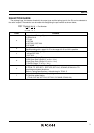
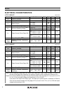
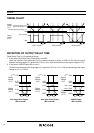
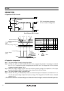
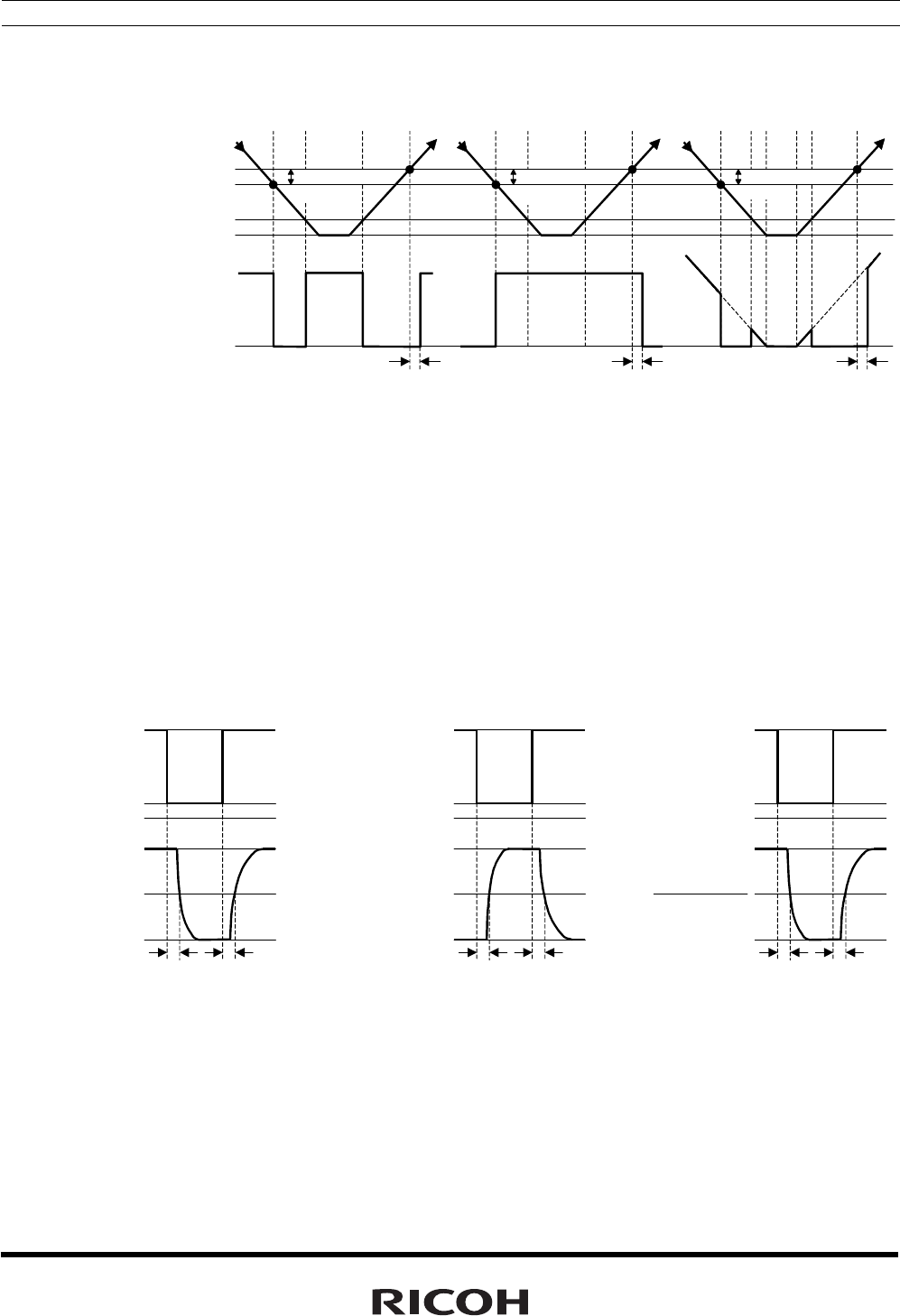
TIMING CHART
Detector Threshold
t
PLH
t
PLH
t
PLH
GND
GND
V
DDL
-
V
DET
+V
DET
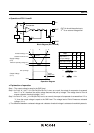
Detector Threshold
Released Voltage
Minimum Operating Voltage
Pull-up Voltage
Supply
Voltage
(V
DD
)
Output
Voltage
(V
OUT
)
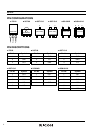
R3111xxxxA R3111xxxxB R3111xxxxC
Detector Threshold Detector Threshold
Hysteresis Hysteresis Hysteresis
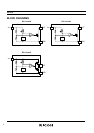
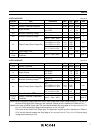
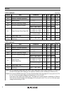
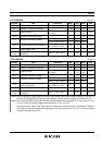
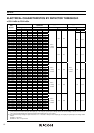
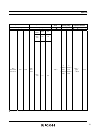
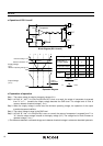
DEFINITION OF OUTPUT DELAY TIME
Output Delay Time (tPLH) is defined as follows:
1. In the case of Nch Open Drain Output:(R3111xxxxA/B)
Under the condition of the output pin (OUT) is pulled up through a resistor of 470kΩ to 5V, the time interval
between the rising edge of V
DD pulse from 0.7V to (+VDET)+2.0V and becoming of the output voltage to 2.5V.
2. In the case of CMOS Output:(R3111xxxxC)
The time interval between the rising edge of V
DD pulse from 0.7V to (+VDET)+2.0V and becoming of the output
voltage to ((+V
DET)+2.0V)/2.
+V
DET
+2.0V
0.7V
Supply
Voltage
(V
DD
)
GND
5.0V
2.5V
GND
Output
Voltage
(V
OUT
)
t
PLH
t
PHL
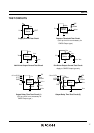
+V
DET
+
2.0V
0.7V
GND
5.0V
2.5V
GND
t
PLH
t
PHL
Supply
Voltage
(V
DD
)
Output
Voltage
(V
OUT
)
+
V
DET
+2.0V
0.7V
GND
GND
t
PLH
t
PHL
+
V
DET
+2.0V
+
V
DET
+2.0V
2
Supply
Voltage
(V
DD
)
Output
Voltage
(V
OUT
)
Nch Open Drain Output Nch Open Drain Output CMOS Output
(R3111xxxxA) (R3111xxxxB) (R3111xxxxC)