


ASUS P2V User’s Manual 45
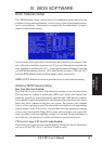
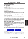
IV. BIOS SOFTWARE
IV. BIOS
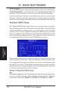
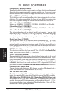
Chipset Features
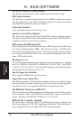
PCI to DRAM Prefetch (Disabled)
Leave on default setting for best stability.
Byte Merge (Disabled)
Leave on default setting for compatibility. Set to Enabled for increased performance
in some PCI VGA cards.
DRAM Read Latch Delay (1.0 ns)
This controls the timing point for latching SDRAM data. Leave on default setting.
MD to HD Delay (Auto)
This controls the pipe stage for SDRAM data MD to host side data bus HD. Leave
on default setting.
DRAM Operating Frequency (Auto)
This controls the DRAM’s operating frequency as that (FSB) or 2/3 (2/3 FSB) of the
host side frequency. Leave on default setting.
AGP Capability (2X Mode)
Leave on default setting for best performance. Set to 1X Mode for compatibility.
Graphics Aperture Size (64MB)
Memory-mapped, graphics data structures can reside in a Graphics Aperture. Leave
on default setting.
Video Memory Cache Mode (UC)
USWC (uncacheable, speculative write combining) is a new cache technology for the
video memory of the processor. It can greatly improve the display speed by caching
the display data. You must leave this on the default setting of UC (uncacheable) if your
display card cannot support this feature or else your system may not boot.
Memory Hole At 15M–16M (Disabled)
Enabling this feature reserves 15MB to 16MB memory address space to ISA expan-
sion cards that specifically require this setting. This makes the memory from 15MB
and up unavailable to the system. Expansion cards can only access memory up to
16MB. This is Disabled by default.
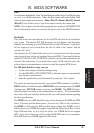
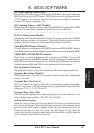
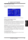
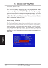
DRAM are xx bits wide
If all your DRAM modules have ECC chips (e.g., 8 chips + 1 ECC chips), they are
considered 72bits and the corresponding screen (left) will be shown. On the other
hand, if your DRAM modules do not have ECC chips (e.g. 8 chips), they are consid-
ered 64 bits and the corresponding screen (right) will be shown.
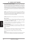
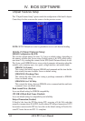
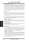
Data Integrity Mode (Non-ECC)
Non-ECC has byte-wise write capability but no provision for protecting data integ-
rity in the DRAM array. EC-Only data errors are detected but not corrected. ECC
allows detection of single-bit and multiple-bit errors and recovery of single-bit er-
rors. (See section III for more information on DRAM memory modules.)
....................................................................................................................................