


ASUS P2V User’s Manual44
IV. BIOS SOFTWARE
IV. BIOS
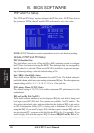
Chipset Features
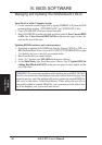
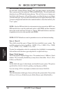
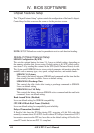
Chipset Features Setup
This “Chipset Features Setup” option controls the configuration of the board’s chipset.
Control keys for this screen are the same as for the previous screen.
NOTE: SETUP Defaults are noted in parenthesis next to each function heading.
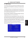
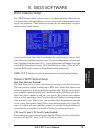
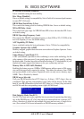
Details of Chipset Features Setup
SDRAM Configuration (By SPD)
This sets the optimal timing for items 2-4. Leave on default setting, depending on
the memory modules that you are using. Default setting is By SPD, which config-
ures items 2-4 by reading the contents in the SPD (Serial Presence Detect) device.
This 8-pin serial EEPROM device stores critical parameter information about the
module, such as memory type, size, speed, voltage interface, and module banks.
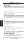
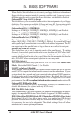
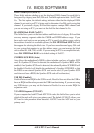
SDRAM CAS Latency
This controls the latency between SDRAM read command and the time that the
data actually becomes available. Leave on default setting.
SDRAM RAS Precharge Time
This controls the idle clocks after issuing a precharge command to SDRAM.
Leave on default setting.
SDRAM RAS to CAS Delay
This controls the latency between SDRAM active command and the read/write
command. Leave on default setting.
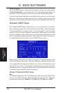
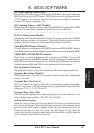
Read Around Write (Disabled)
Leave on default setting for SDRAM compatibility.
CPU-DRAM Back-Back Trans. (Disabled)
Leave on default setting for compatibility and reliability.
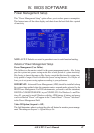
Delayed Transaction (Enabled)
If Enabled, this frees the PCI Bus during CPU accessing of 8-bit ISA cards that
normally consume about 50–60 PCI clocks without PCI delayed transaction. If PCI
bus masters cannot use the PCI bus, leave this on the default setting of Disabled for
some PCI cards that are not PCI 2.1 compliant.