


GM862-GPS Hardware User Guide
1vv0300728 Rev. 0 - 27/04/06
Reproduction forbidden without Telit Communications S.p.A. written authorization - All Right reserved page 11 of 55
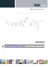
3.2 General Design Rules
The principal guidelines for the Power Supply Design embrace three different design steps:
- the electrical design
- the thermal design.
- the PCB layout.
3.2.1 Electrical design Guidelines
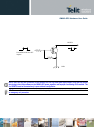
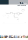
The electrical design of the power supply depends strongly from the power source where this power is
drained. We will distinguish them into three categories:
• +5V input (typically PC internal regulator output)
• +12V input (typically automotive)
• Battery
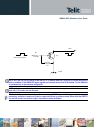
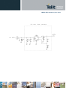
3.2.1.1 + 5V input Source Power Supply Design Guidelines
• The desired output for the power supply is 3.8V, hence there's not a big difference between the
input source and the desired output and a linear regulator can be used. A switching power supply
will not be suited because of the low drop out requirements.
• When using a linear regulator, a proper heat sink shall be provided in order to dissipate the power
generated.
• A Bypass low ESR capacitor of adequate capacity must be provided in order to cut the current
absorption peaks close to the GM862-GPS, a 100μF tantalum capacitor is usually suited.
• Make sure the low ESR capacitor on the power supply output (usually a tantalum one) is rated at
least 10V.
• A protection diode should be inserted close to the power input, in order to save the GM862-GPS
from power polarity inversion.