


12
LA000507G © 2006 Navman New Zealand. All rights reserved. Proprietary information and specications subject to change without notice.
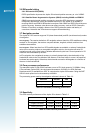
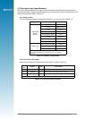
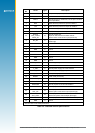
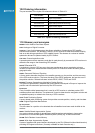
Pad
No.
Name Type Description
1 PWRIN P main power input (3.3 V)
2 GND P ground
3 BOOT I
serial boot (high for serial boot, low or open circuit for
normal operation)
4 RXA I CMOS level asynchronous input for UART A
5 TXA O CMOS level asynchronous output for UART A
6 TXB O CMOS level asynchronous output for UART B
7 RXB I CMOS level asynchronous input for UART B
8*
GPIO3/
ADC_CONV/
NANT_SC
IO
general purpose IO/
output for external A/D converter control/
antenna short circuit sensor input (active low)
9 RF_ON O
output to indicate whether the RF section is enabled
(active high)
10 GND P ground
11 GND P ground
12 GND P ground
13 GND P ground
14 GND P ground
15 GND P ground
16 GND P ground
17 RF_IN I antenna signal input
18 GND P ground
19 V_ANT P external power supply for active antenna
20 VCC_RF O RF Power (+2.8 V) supply output
21 V_BATT P backup battery input
22 RESET I master reset (active low)
23 GPIO10/GPS_FIX IO general purpose IO or GPS x indication (active low)
24 GPIO6/SDO IO general purpose IO or SPI serial data out
25 GPIO5/SDI IO general purpose IO or SPI serial data in
26 GPIO7/SCK IO general purpose IO or SPI serial clock
27*
GPIO15/
ANT_OC
IO
general purpose IO/
antenna open circuit sensor input (active high)
28*
GPIO1/
ANT_CTRL
IO
general purpose IO/
antenna DC power control output (ON=high)
29 GPIO9/1PPS O general purpose IO or 1 pulse per second output
30 GND P ground
* See also Table 4‑4 for J20D pad functions
Table 4-5: J20/J20S receiver pad functions