


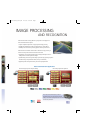
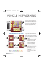
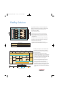
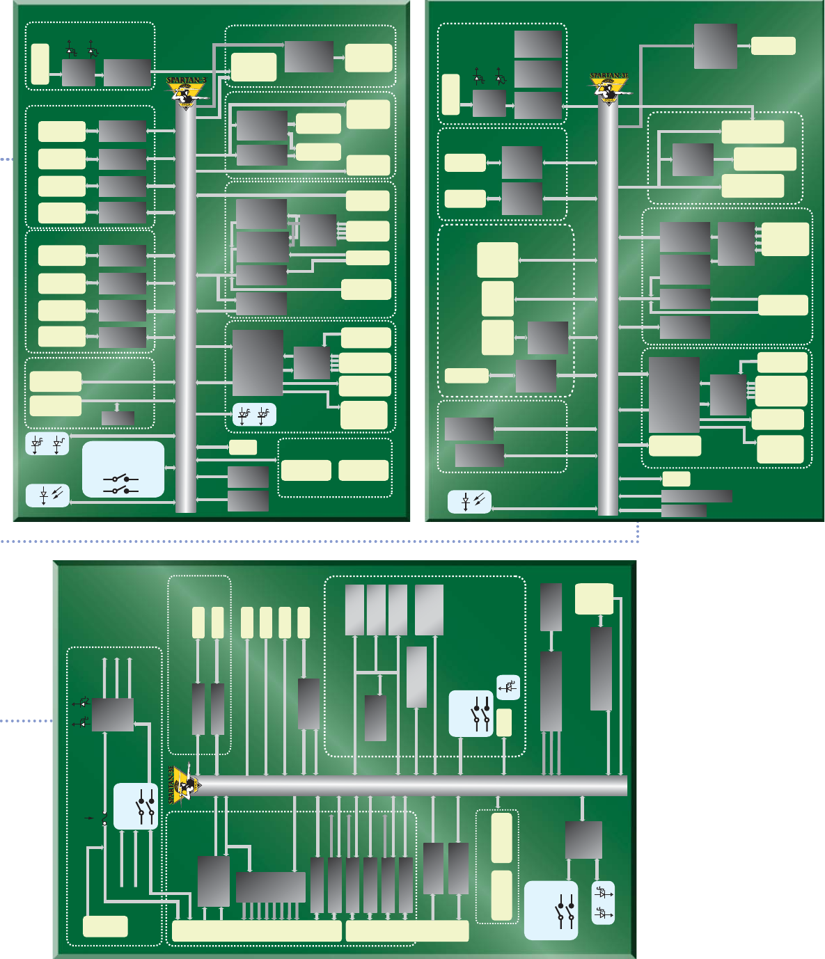
Power Supply
Vehicle Connectivity
Voltage
Indicators
Board
PSU
COG PSU &
Sequencing
MOST IDT
PLL
2x
CAN PHY
2x
LIN PHY
FlexRay
PHY
Application Connectivity
Debug App.
RS232 PHY
Ethernet
PHY
USB OTG
PHY
Firewire
PHY
Memory and Configuration
CPLD
8 x LED
Remote Control
Switches
5 Push Buttons or 5x5
Key Matrix 8 DIP SW
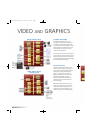
Video Out 3
2 x
Touch Screen
Video Out 1 & 2
2 x VGA DAC,
Analog RGB
2 x DVI Tx
Video IN 1 & 2
2 x Video
Decoder
Video
MUX 4x2
2 x VGA ADC,
Analog
RGB
Video CLK
PLL
2 x DVI Rx
Audio
1/2 Stereo
CODEC ADC
1/2 Stereo
CODEC DAC
Stereo
Audio
MUX 4x2
2 x IR Stereo
Audio Channels
RST Ctrl.
OSC
33MHz
User Expansion Header
logiCRAFT2
PSU Conn
MOST
FOT
2 x DB9
Male
2 x DB9
Male
DB9
Male
DB9
Female
RJ45
MiniA/B
2x
Firewire
128MB/64-bit
DDRAM
8MB/16-bit
NOR Flash
Dia. RGB &
COG Ctrl.
Hirose DF11
2 x Resistive
Touch Screen
Conn.
2 x S-Video
CVBS
2 x DVI
2 x LVDS
Hirose DF11
2 x Digital
RGB
Hirose DF11
1 x LVDS
Hirose DF11
2 x S-Video
(4xCVBS)
2 x DVI
Digital RGB
Hirose FX2-60
2 x Mono Mic
Micro Jack
4 x Stereo Line
IN Micro Jack
2 x Stereo Line
Out Micro Jack
2 x Stereo
Headphones
Micro Jack
Hirose FX2-60
40 FPGA IOB
Hirose FX2-60
40 FPGA IOB
JTAG
3S1500
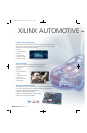
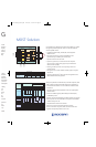
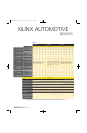
Automotive Grade Power Supply
Vehicle
Connectivity
Voltage
Indicators
Various Board
Supply Voltages
Board
PSU’s
High and Low
Side Switch
Inputs
High
and
Low
Side
Drivers
Switches
4 Push Buttons
or 8 DIP SW
Application Connectivity
Ethernet PHY
USB 2.0 PHY
User Expansion Header
XA1600E
External
Power Input
Vehicle Connection Port
D-SUB 44 Pin Male
Vehicle Connection Port
D-SUB 44 Pin Male
RJ45
RJ45
2x SMA
External
Clock
Socket
DIL8
160 Pin Molex
Connector
160 Pin Molex
Connector
JTAG
3S1600E
WAKEUP
JUMPERS
FUSE
WAKE CAN
WAKE LIN
VOLT1
VOLT2
VOLTX
WAKE BOARD
VEHICLE BATT
VEHICLE IGN
WAKE
DETECT
SPI
HS
HS
HS
HS
LS
LS
LS
LS
PWM IN
2x FlexRay PHY
HS CAN PHY
HS CAN PHY
LS CAN PHY
2x LIN PHY
K-Line PHY
16 ch 1 MSPS
12-bit A/D
Debug App.
RS232 PHY
16 CH
WAKE CAN
WAKE CAN
WAKE LIN
12 x LED
Port
Extender
LVDS TX DIFFERENTIAL PAIR
2x SMA
LVDS RX DIFFERENTIAL PAIR
2x SMA
LVDS CLK DIFFERENTIAL PAIR
2x SMA
LVDS CLK
LVDS CLK
SYNTHESIZER
SPI CONFIG
Memory and Configuration
1MB/16-bit
SRAM
32MB/32-bit
SDRAM
Xilinx Config
FLASH
8Mbit/16-bit
Serial NOR Flash
32 Mbit (4M x 8)
8MB/16-bit
NOR Flash
9536XL
CPLD
DATA/ADDRESS BUS
SPI
SLAVE PARALLEL (8 BIT)
CONFIG
MODE
Config Options:
– SPI
– Slave Parallel
Config Indicators
User Configurable PLL OSC 24MHz
SPI
PLL Config
CLK1
2C256 CPLD
CLK2
CPLD:
– Level Shifting
– Configuration
– Wake-up
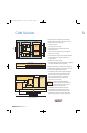
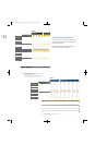
Power Supply
Vehicle Connectivity
Video Out 1
Application Connectivity
Memory and Configuration
Voltage
Indicators
COG PSU &
SEQUENCING
LED
Backlight PSU
COG VCOM
GAMMA PSU
Video IN 1 & 2
Video
Decoder
Video
Decoder
Video
Amplifier
and
MUX 4x2
Video CLK
PLL
LVDS
Transceiver
Remote Control
logiCRAFT3
Digital RGB
Hirose FX2-60
Audio
Stereo
Audio
Amplifier
MUX 4x2
Mono Mic
PCB Pad
4x Stereo Line
IN 4x RCA and
4vx PCB Pads
Stereo Line
Out PCB Pad
2 x IR Stereo
Ch. Hirose DF11
Stereo
Headphones
PCB Pad
1/2 Stereo
CODEC ADC
1/2 Stereo
CODEC DAC
RST Ctrl.
OSC 33MHz
JTAG
Board
PSU
PSU Conn
Hirose DF11
CAN
PHY
DB9 Male
CAN
PHY
CVBS
Encoder
DB9 Male
3S250E, 3S500E or 3S1200E
Dig. RGB & COG
Ctrl. Hirose DF11
S-Video CVBS
2xRCA
LVDS
Hirose DF11
2x S-Video,
(4xCVBS)
4 x RCA
5 Pin .1”
single row
header
To iPod
Hirose
DF11
Hirose
DF11
To
Bluetooth
Module
DB9 Female
BPI Config
8 GPIO’s
16MB/32-bit
SDRAM
8MB/8-bit
NOR Flash
GPIO
Extender
Debug App.
RS23
PHY
Touch
Screen
Auto.Brochure_Final.qxd 12/19/07 9:19 AM Page 7