


C8051F04x-DK
8 Rev. 0.6
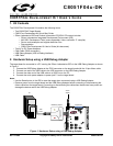
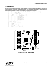
6.1. System Clock Sources
The
C8051F040
device installed on the target board features a calibrated programmable internal oscillator which is
enabled as the system clock source on reset. After reset, the internal oscillator operates at a frequency of
3.0625 MHz (±2%) by default but may be configured by software to operate at other frequencies. Therefore, in many
applications an external oscillator is not required. However, an external 22.1184 MHz crystal is installed on the target
board for additional applications. Refer to the
C8051F04x
data sheet for more information on configuring the system
clock source.
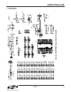
6.2. Switches and LEDs
Two switches are provided on the target board. Switch SW1 is connected to the RESET pin of the C8051F040.
Pressing SW1 puts the device into its hardware-reset state. Switch SW2 is connected to the C8051F040’s general
purpose I/O (GPIO) pin through headers. Pressing SW2 generates a logic low signal on the port pin. Remove the
shorting block from the header to disconnect SW2 from the port pins. The port pin signal is also routed to a pin on
the J24 I/O connector. See Table 1 for the port pins and headers corresponding to each switch.
Two LEDs are also provided on the target board. The red LED labeled PWR is used to indicate a power connection
to the target board. The green LED labeled with a port pin name is connected to the C8051F040’s GPIO pin
through headers. Remove the shorting block from the header to disconnect the LED from the port pin. The port pin
signal is also routed to a pin on the J24 I/O connector. See Table 1 for the port pins and headers corresponding to
each LED.
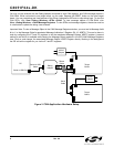
6.3. Target Board JTAG Interface (J4)
The
JTAG
connector (J4) provides access to the
JTAG
pins of the C8051F040. It is used to connect the Serial
Adapter or the USB Debug Adapter to the target board for in-circuit debugging and Flash programming. Table 2
shows the
JTAG
pin definitions.
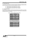
Table 1. Target Board I/O Descriptions
Description I/O Header
SW1 Reset none
SW2 P3.7 J1
Green LED P1.6 J3
Red LED PWR none
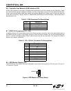
Table 2. JTAG Connector Pin Descriptions
Pin # Description
1 +3VD (+3.3VDC)
2, 3, 9 GND (Ground)
4TCK
5TMS
6TDO
7TDI
8, 10 Not Connected