


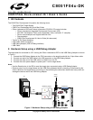

C8051F04x-DK
10 Rev. 0.6
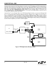
6.6. Controller Area Network (CAN) Interface (J25)
A DB-9 (J25) connector is provided to facilitate serial connections to the CAN interface on the C8051040. In addi-
tion, when a shorting block is installed on header J7, writing a logic 'high' to port pin P4.2 will place the CAN trans-
ceiver in low-current standby mode. Also, resistor R12 may be replaced with a higher value to control the slew rate
of the CAN_H and CAN_L signals. See the TI SN65HVD230 data sheet for further information. Table 5 listes the pin
descriptions for J25.
6.7. PORT I/O Connectors (J12 - J19)
In addition to all port I/O signals being routed to the 96-pin expansion connector, each of the eight parallel ports of
the C8051F040 has its own 10-pin header connector. Each connector provides a pin for the corresponding port
pins 0-7, +3.3VDC and digital ground. Table 6 defines the pins for the port connectors. The same pin-out order is
used for all of the port connectors.
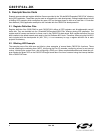
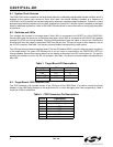
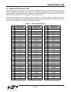
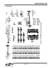
6.8. VDD Monitor Disable (J23)
The VDD Monitor of the C8051F040 may be disabled by moving the shorting block on J23 from pins 1–2 to pins 2–
3, as shown in Figure 4.
Figure 4. VDD Monitor Hardware Setup
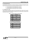
Table 5. CAN Connector Pin Descriptions
Pin # Description
2CAN_L
7CAN_H
3, 6 GND (Ground)
1, 4, 5, 8, 9 Not Connected
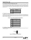
Table 6. J12- J19 Port Connector Pin Descriptions
Pin # Description
1Pn.0
2Pn.1
3Pn.2
4Pn.3
5Pn.4
6Pn.5
7Pn.6
8Pn.7
9 +3VD (+3.3VDC)
10 GND (Ground)
1
3
2
MONEN