


C8051F04x-DK
Rev. 0.6 7
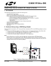
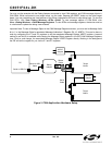
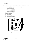
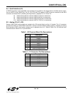
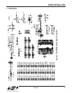
6. Target Board
The
C8051F04x
Development Kit includes a target board with a
C8051F040
device pre-installed for evaluation and
preliminary software development. Numerous input/output (I/O) connections are provided to facilitate prototyping
using the target board. Refer to
Figure 3
for the locations of the various I/O connectors.
P1 Power connector (accepts input from 7 to 15 VDC unregulated power adapter)
J1 Connects SW2 to P3.7 pin
J3 Connects LED D3 to P1.6 pin
J4 JTAG connector for Debug Adapter interface
J5 DB-9 connector for UART0 RS232 interface
J6 Connector for UART0 TX (P0.0)
J8 Connector for UART0 RTS (P4.0)
J9 Connector for UART0 RX (P0.1)
J10 Connector for UART0 CTS (P4.1)
J11 Analog loopback connector
J12-J19 Port 0 - 7 connectors
J20 Analog I/O terminal block
J22 VREF connector
J23 VDD Monitor Disable
J24 96-pin Expansion I/O connector
J25 DB-9 connector for CAN interface
Figure 3. C8051F040 Target Board
J24
Port 1
Port 2
Port 3
Port 0
Port 7
Port 6
Port 5
Port 4
Pin 1
J20
JTAG
Pin 1
J25 J5
J1
CAN RS232
RESET
P3.7
J9
J6
J10
J8
J3
J23J7
C8051
F04X
J2
J21
J22
Pin 1
Pin 2
J11
Pin 1
Pin 2
P1.6
Pin 1
PWR
P1
J4