


3.0 Quick Start
2. Perform steps 2 and 3 of stand alone quick start,,
above.
Note: To develop the ADC clock, the Digital Interface
Board divides its on-board clock. In doing so, jitter is
introduced to the ADC clock which degrades the
observed performance of the ADC12040. See Section
6.0 Obtaining Best Results for an explanation of this
phenomenon and how to avoid it.
3. Use of the crystal oscillator located at Y1 is
recommended to clock the ADC. To do so, connect
the jumper at JP2 to pins 2 and 3. This is the default
position. The ADC clock signal may be monitored at
TP7. Because of clock isolation resistor R12 and the
scope probe capacitance, the clock signal at TP7
will appear integrated.
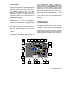
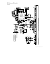
Refer to Figure 1 for locations of test points and major
components. For Stand-Alone operation:
4. Perform steps 5 through 7 of the Stand-Alone quick
start, above.
1. Install an appropriate crystal into socket Y1. While
the oscillator may be soldered to the board, using a
socket will allow you to easily change clock
frequencies.
5. See the Digital Interface Board Manual for
instructions for setting the ADC clock frequency and
for gathering data.
2. Connect a clean power supply to Power Connector
P1. Supply +5V at pin 3 of P1 to supply the Digital
Interface board. Supply +3.3V to pin 1 for the
ADC12L063, or +5V to pin 1 for the ADC12010,
ADC12020 and the ADC12040. Pin 2 is ground.
4.0 Functional Description
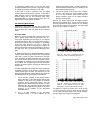
The ADC12040 Evaluation Board schematic is shown in
Figure 6.
3. Use VR1 to set the reference voltage (V
REF
), which
is 2.0V for the ADC12040, ADC12010, or
ADC12020, or to 1.0V for the ADC12L063. V
REF
can be measured at TP1.
4.1 Input (signal conditioning) circuitry
The input signal to be digitized should be applied to BNC
connector J1. This 50 Ohm input is intended to accept a
low-noise sine wave signal of 2V peak-to-peak amplitude
for the ADC12040, ADC12010 and ADC12020 or 1V
peak-to-peak for the ADC12L063. To accurately evaluate
the dynamic performance of these converters, the input
test signal will have to be passed through a high-quality
bandpass filter with at least 14-bit equivalent noise and
distortion characteristics.
4. To use the crystal oscillator located at Y1 to clock
the ADC, connect the jumper at JP2 to pins 2 and 3.
This is the default position. The ADC clock signal
may be monitored at TP7. Because of clock
isolation resistor R12 and the scope probe
capacitance, the clock signal at TP7 will appear
integrated.
5. Connect the jumper at JP3 between pins 1 and 2,
and the jumper at JP4 to pins 1 and 2 to select input
J1 only. This is the default position.
Signal transformer T1 provides single-ended to
differential conversion. The common mode voltage at the
ADC input is equal to the reference voltage of the ADC.
6. Connect a signal of 1.4 V
P-P
amplitude for the
ADC12040, ADC12010 or the ADC12020, or 0.7
V
P-P
for the ADC12L063 from a 50-Ohm source to
Analog Input BNC J1. The ADC input signal can be
observed at TP5. Because of isolation resistor R18
and the scope probe capacitance, the input signal at
TP5 may not have the same frequency response as
the ADC input. Be sure to use a bandpass filter
before the Evaluation Board.
No scope or other test equipment should be connected to
TP3 or to TP4 while gathering data.
This evaluation board is capable of accommodating a
single input or two different inputs. These inputs are NOT
differential in nature, but are intended to mix two different
signals before presenting them to the ADC.
NOTE: If input frequency components above 30
MHz are required, remove capacitor C7 at the ADC
differential input pins.
7. Adjust the input signal amplitude as needed to
ensure that the signals at TP3 and TP4 remains
within the valid signal range of 0V to V
REF
.
4.1.1 Single Input
8. The digitized signal is available at pins B16 through
B21 and C16 through C21 of J2. See board
schematic of Figure 6.
To evaluate the ADC12040 with a single input, connect
jumpers JP3 and JP4 in their default positions, as shows
in Figure 1. That is, short together pins 1 and 2 of JP3
and of JP4. Doing so provides a 50-Ohm input at J1. No
connection should be made to J3. This configuration is
appropriate for evaluation of dynamic performance
parameters.
For Computer Mode operation:
NB: Be sure to read section 6.1 before using this
board in the Computer Mode.
1. Connect the evaluation board to the Digital Interface
Board. See the Digital Interface Board Manual for
operation of that board.
4 http://www.national.com