


190-00228-20 GPS 16/17 Technical Specifications Rev. C
Page 8
2 GPS 16/17 WIRING AND PINOUTS
2.1 GPS 16/17 Pinout
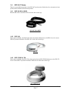
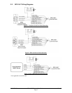
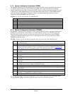
The GPS 16LVS, GPS 16HVS, and GPS 17HVS sensors utilize an 8-pin RJ-45 plug. The GPS 16A and
GPS 17N feature a stripped and pre-tinned, 5-wire cable assembly for connection flexibility. The following
is a functional description of each wire in the cable assembly.
RJ-45
Pin
#
Wire
Color
Signal
Name
Description
1 Red POWER GPS 16LVS: Regulated +3.3 to +6 VDC. Typical operating current is 80 mA. An
internal 6.8 V transient zener diode and a positive temperature coefficient
thermistor protect from transients and over-voltages. With voltages greater than
6.8 VDC the zener will draw several amps of current through the thermistor,
causing it to heat rapidly and eventually power the unit off, unless an external
fuse blows first. When proper supply voltages are returned, the thermistor will
cool and allow the GPS 16LVS to operate. The CMOS/TTL output buffers are
powered by Vin; therefore, a 3.3 VDC supply will create 3.3 V logic output
levels.
GPS 16HVS, GPS 16A, GPS 17HVS, & GPS 17N: Vin can be an unregulated
6.0 VDC (8.0 VDC for GPS 16A and GPS 17N) to 40 VDC, optimized for 12
VDC. Typical operating power is 800 mW. This voltage drives a switching
regulator with a nominal 5.0 VDC output, which powers the internal linear
regulators, and the CMOS output buffers.
2 Black GROUND Power and Signal Ground
3 Yellow REMOTE
POWER
ON/OFF
(N/A for GPS 16A) External Power Control Input. Active (ON) if less than 0.3
VDC. Inactive (OFF) if open-circuit. 51 kΩ internal pull-up resistor to the
voltage on the POWER input. Activation of this input powers the internal
regulators off and drops the supply current below 20mA in the GPS 16LVS, and
below 1 mA in the GPS 16HVS, GPS 17HVS, and GPS 17N. This input is
intended to be driven by an open-collector output.
4 Blue PORT 1
DATA IN
First Serial Asynchronous Input. RS-232 compatible with maximum input
voltage range -25 < V < 25. This input may also be directly connected to standard
3 to 5 VDC CMOS logic. The low signal voltage requirement is < 0.9 V, and the
high signal voltage requirement is > 2.1 V. Maximum load impedance is 4.7 kΩ.
This input may be used to receive serial initialization/ configuration data as
specified in Section 4.1
Received NMEA 0183 Sentences.
5 White PORT 1
DATA
OUT
First Serial Asynchronous Output. This RS-232 compatible (TTL level on GPS
16A and GPS 17N) output normally provides serial data which is formatted per
NMEA 0183, Version 3.0. This output is also capable of outputting phase data
information, see Appendix C for details. The NMEA 0183 baud rate is switchable
in the range of 300 to 19200 baud (38400 for GPS 16A). The default baud rate is
19200 for GPS 16A and 4800 for all other products.
6 Gray PPS (N/A for GPS 16A and GPS 17N) One-Pulse-Per-Second Output. Typical voltage
rise and fall times are 300 ns. Impedance is 250 Ω. Open circuit output voltage is
low=0 V and high=Vin in the GPS 16LVS, and low=0 V and high=5.0 V in the
GPS 16HVS and GPS 17HVS. The default format is a 100 ms wide active-high
pulse at a 1 Hz rate; the pulse width is configurable in 20 ms increments. Rising
edge is synchronized to the start of each GPS second. This output will provide a
nominal 700 mVp-p signal into a 50 Ω load. The pulse time measured at the 50%
voltage point will be about 50 ns earlier with a 50 Ω load than with no load.
7 Green PORT 2
DATA IN
Second Serial Asynchronous Input, electrically identical to PORT 1 DATA IN.
This input may be used to receive serial differential GPS data formatted per
RTCM SC-104 Recommended Standards For Differential Navstar GPS Service,
Version 2.2 (see Section 4.5
Received RTCM Data for details).
8 Violet PORT 2
DATA
OUT
(N/A for GPS 16A) Second Serial Asynchronous Output, electrically identical to
PORT 1 DATA OUT. Reserved for future use.
Table 1: GPS 16/17 Wire Pinout