


Page 6 GPS 15 TECHNICAL SPECIFICATIONS
Rev. A P/N 190-00266-00
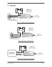
2 PINOUT
2.1 DESCRIPTION
The GPS 15-F utilizes a six-pin LIF connector. The GPS 15-W utilizes a six-pin JST connector with
mating wire harness included.
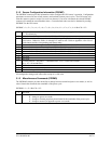
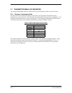
Table 1. Signal/Wire Descriptions
GPS
15
Pin #
Signal Name Description
1 BACKUP POWER This input provides external power to maintain the battery-backed SRAM
and real-time clock. This enables the user to provide backup power if
needed for longer than the optional on-board backup battery will provide
(roughly 21 days). Input voltage must be between +2.8 and +3.4 Vdc.
2 GROUND Power and Signal Ground
3 POWER Regulated +3.3 Vdc input. Peak operating current is 85 mA. Nominal
operating current is 80 mA.
4 PORT 1 DATA OUT Serial Asynchronous Output.
CMOS compatible output designed to interface directly with a host
microprocessor. Provides serial data which is formatted per “NMEA 0183,
Version 3.0”. The baud rate is set during production to 4800, but other rates
are available.
5 PORT 1 DATA IN First Serial Asynchronous Input.
CMOS compatible input designed to interface directly with a host
microprocessor. Maximum input voltage range of 0 < V < 3.3.
6 RF BIAS This input allows the user to externally apply a RF bias to the active
antenna. Units are shipped with this feature disabled. By default, the unit
will use an internal voltage to power the active antenna.