


5
5
4
4
3
3
2
2
1
1
E E
D D
C C
B B
A A
nRESET
nRESET
nRESET
USB5V
VOUT
VADC
12V 3V3
3V3
3V3
EXT3V3
EXT3V3USB5V 12V
3V3
VBATT
VBATT
3V3
3V3
JTDO
nSTDBYO
JTDI
JTMS
JTCK
nRESET
nJTRST
nSTDBYI
BOOTEN
USBOE
STDBYIN_WAKEUP
AIN1
AIN2
AIN3
AIN0
Mod15_rsvd
Mod14_rsvd
PPS
Mod13_rsvd
Wakeup
GPIO3_A
USBDP
GPIO2_A
USBDN
GPIO2_B GPIO3_B
GPIO0 GPIO1
UART0RX
UART1TX
UART0TX
TRACKLED
Wakeup
Mod36_rsvd
UART1RX
Mod37_rsvd
USBRST
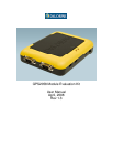
Title
Size Document Number Rev
Date: Sheet
of
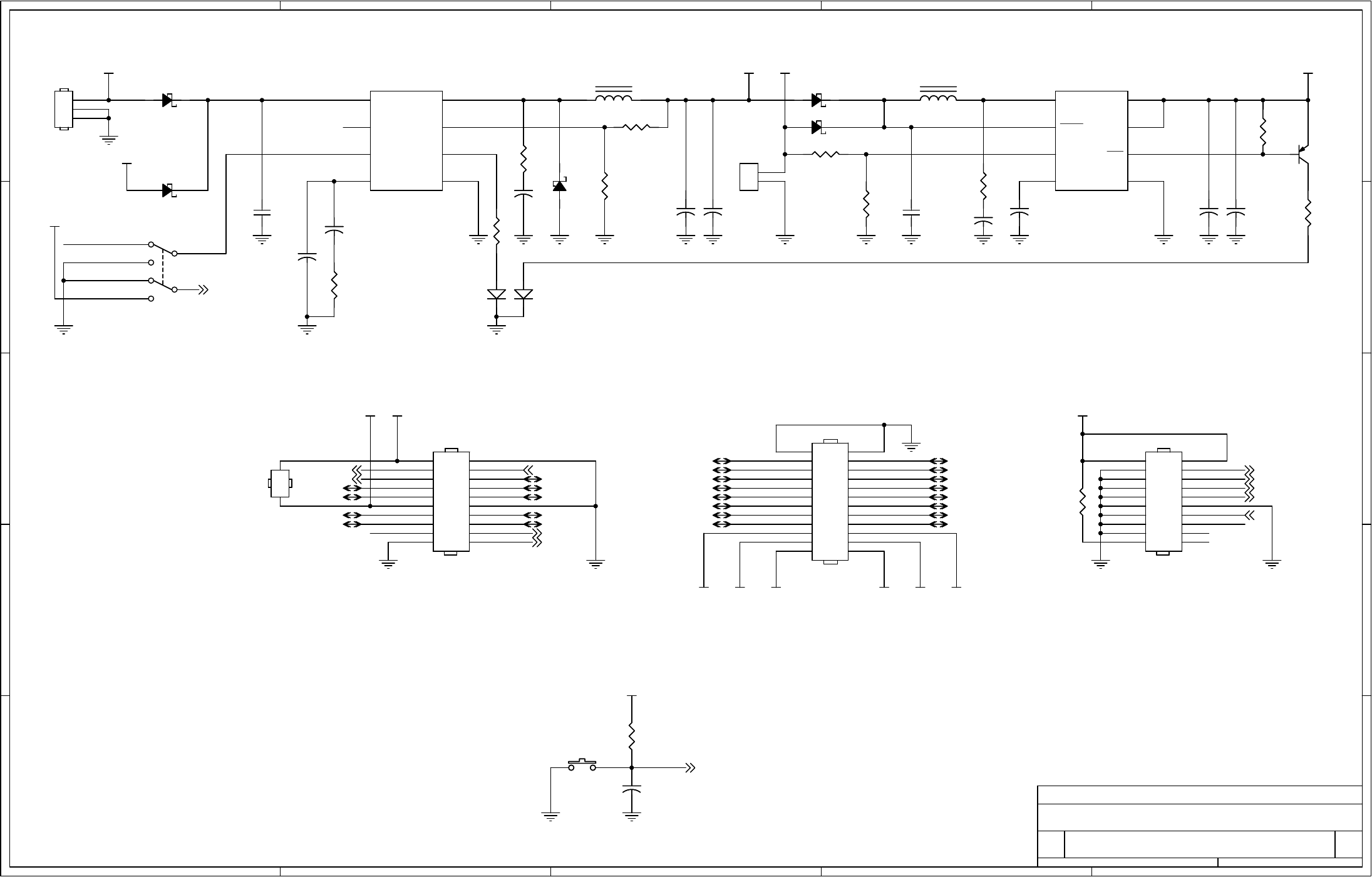
DeLORME_GPS_MODULE_EVK1_SCHEMATIC C
DeLorme GPS Module Evaluation Kit, Main Power and Connectors page
B
12Wednesday, April 23, 2008
Title
Size Document Number Rev
Date: Sheet
of
DeLORME_GPS_MODULE_EVK1_SCHEMATIC C
DeLorme GPS Module Evaluation Kit, Main Power and Connectors page
B
12Wednesday, April 23, 2008
Title
Size Document Number Rev
Date: Sheet
of
DeLORME_GPS_MODULE_EVK1_SCHEMATIC C
DeLorme GPS Module Evaluation Kit, Main Power and Connectors page
B
12Wednesday, April 23, 2008
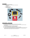
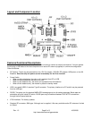
Low ESR
POWER LED:
GREEN = DC On, Battery Good
YELLOW = DC On, Battery Low
RED = No DC, Battery Low
Low ESR
On/Wakeup
Off/Standby
DeLorme, Yarmouth, ME drawn by JP/Hardware
JTAG Port20-pin developer's connector 24-pin developer's connector
1%
1%
When batteries are present, the main
switch operates as Wakeup-Standby.
Without batteries, it acts as On-Off.
J12 provides an easy way to
access the VADC and 3V3
supplies but should not
be jumpered.
Connectors J4, J5 and J6 are shown as oriented in the evaluation kit.
Note: GPIO2_A/B & GPIO3_A/B are selected
from J10A (left module connector) and J10B
(right module connector) via switch on GPS2058
module adaptor card; switch-down selects
GPIOx_A and switch-up selects GPIOx_B
R3
3K3
R3
3K3
U1
E-L5970D
U1
E-L5970D
Vcc
8
OUT
1
GND
7
FB
5
VREF
6
SYNC
2
COMP
4
INH
3
L1
22uH
L1
22uH
R5
100K
R5
100K
R38
100
R38
100
SW2
Pushbutton_RESET
SW2
Pushbutton_RESET
D3 MA2YD2100LD3 MA2YD2100L
L2
15uH
L2
15uH
D4 MA2YD2100LD4 MA2YD2100L
D2
MA2YD2100L
D2
MA2YD2100L
J1
DC Power Jack
J1
DC Power Jack
3
2
1
+
C8
47uF
+
C8
47uF
R1
4K7
R1
4K7
Q1
2N3906
Q1
2N3906
D1
MA2YD2100L
D1
MA2YD2100L
R4 62KR4 62K
SW1
Main Power Slide Switch
SW1
Main Power Slide Switch
C1
10uF
C1
10uF
C9
1uF
C9
1uF
R7
100
R7
100
C7
0.1uF
C7
0.1uF
R9
10K
R9
10K
C6
10uF
C6
10uF
R6
62K
R6
62K
R8
82
R8
82
R10
10K
R10
10K
D10
MA22D1500L
D10
MA22D1500L
C33
1000pF
C33
1000pF
J12
HEADER 1x2
J12
HEADER 1x2
12
RG
D5
BRPG1211C
RG
D5
BRPG1211C
12
34
C34
1000pF
C34
1000pF
J3
HEADER_10x2_RA
J3
HEADER_10x2_RA
1
3
5
7
9
11
13
15
17
19
2
4
6
8
10
12
14
16
18
20
R2
5K6
R2
5K6
C2
220pF
C2
220pF
J4
HEADER_10x2
J4
HEADER_10x2
1
3
5
7
9
11
13
15
17
19
2
4
6
8
10
12
14
16
18
20
J5
HEADER_12x2
J5
HEADER_12x2
2
4
6
8
10
12
14
16
18
20
22
24
1
3
5
7
9
11
13
15
17
19
21
23
C3
22pF
C3
22pF
+
C4
47uF
+
C4
47uF
C10
0.1uF
C10
0.1uF
J2
2xAA_Coin
J2
2xAA_Coin
1
2
U2
L6920DB
U2
L6920DB
OUT
8
FB
1
LX
7
LBI
2
SHDN
5
REF
4
GND
6
LBO
3
C5
1uF
C5
1uF
R37
100
R37
100