LA000605D © 2007 Navman New Zealand. All rights reserved. Proprietary information and specications subject to change without notice.
3
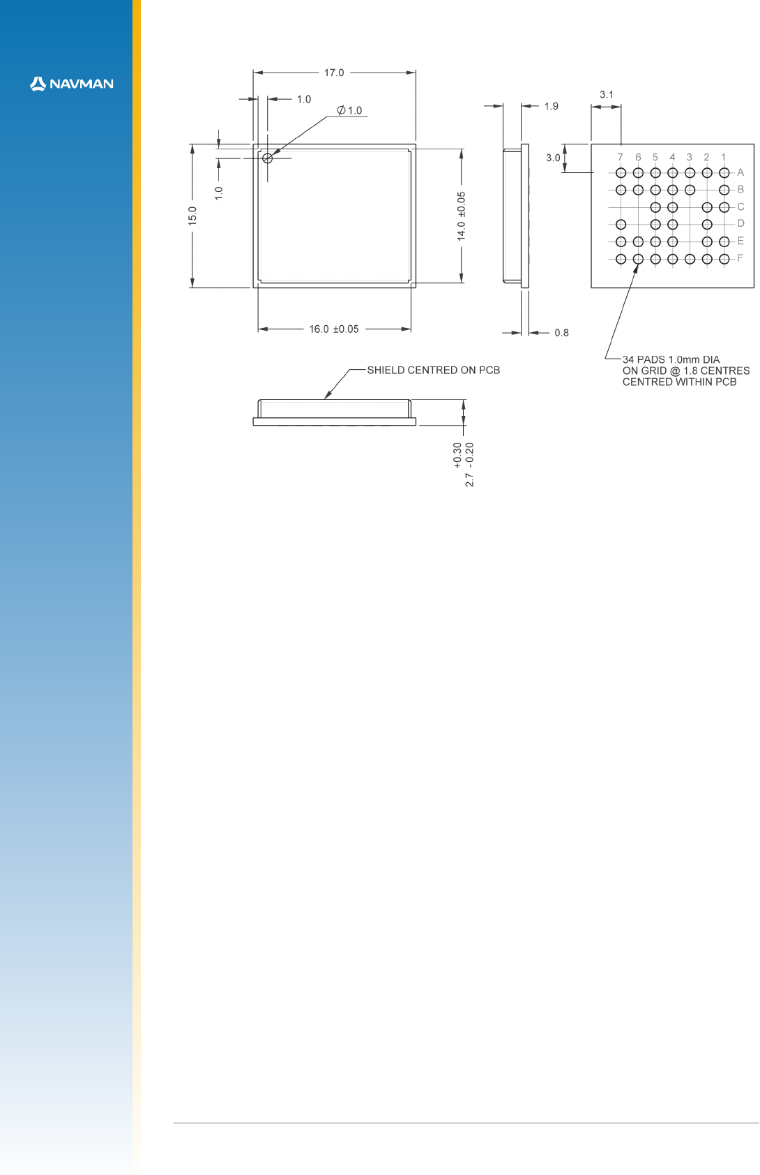
Figure 2-1: Jupiter 32 mechanical layout
2.2 Typical application circuit
The schematic in Figure 2-2 (next page) represents a very basic application circuit, with simple
interfaces to the module. It is subject to variations depending on application requirements.
2.2.1 Power for receiver and active antenna
The receiver power connection requires a clean 3.3 VDC. Noise on this line may affect the
performance of the GPS receiver.
When an active antenna is used, the DC power is fed to it through the antenna coax. This
requires the user to apply the antenna DC voltage to pad A4 of the module.
A 2.85 V 30 mA supply is made available on pad F3 if the chosen antenna can accept that
voltage. This supply is under the command of the TricklePower energy control.
The source impedance of the power supply must be kept sufciently low. The capacitance of
the power supply and PCB track width determine the overall source impedance. If a passive
antenna is used, the supply must be able to provide a minimum of 100mA continuously with
minimal ripple as measured at the power input pin. This ripple requirement must be adhered
to for a larger current ow when an active antenna is used. In-rush current for some active
antennas have been measured as high as 70mA and may cause a dip in voltage or ripple.
Therefore, a low source impedance is important since the power to the Jupiter 32 must be
able to accommodate instantaneous currents in excess of 200mA.
2.2.2 Grounding
Separate analogue and digital grounds are not used. However, the antenna signal ground
uses a particular layout for optimum results. See Figure 2-3 (next page) and Section 2.3.5
for ground plane recommendations and for design considerations involving the antenna input
and the 50 ohm microstrip connection.
All dimensions in mm


