


an appropriate bandpass filter as even the best signal
generator available can not produce a signal pure enough
to evaluate the dynamic performance of an ADC.
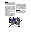
ADC12010 evaluation board, a 20 MHz oscillator for
the ADC12020 evaluation board, or a 60 MHz on the
ADC12L063 evaluation board).
3. Connect the jumper at JP2 to pins 2 and 3 (default
position). This selects the crystal oscillator located
at Y1 on the evaluation board (rather than the
divided oscillator signal on the Digital Interface
Board) to clock the ADC.
If this board is used in conjunction with the Digital
Interface Board and WaveVision software, a cable with a
DB-9 connector must be connected between the Digital
Interface Board and the host computer when using
WAVEVSN BRD 3.0 Digital Interface Board. See the
Digital Interface Board manual for details.
Because the divided signal from the Digital Interface
Board and the oscillator at Y1 are not synchronized, bad
data will sometimes be taken because we are latching
data when the outputs are in transition. This data might
be as you see in Figure 3 or Figure 4.
6.0 Obtaining Best Results
Obtaining the best results with any ADC requires both
good circuit techniques and a good PC board layout. The
layout is taken care of with the design of this evaluation
board.
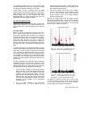
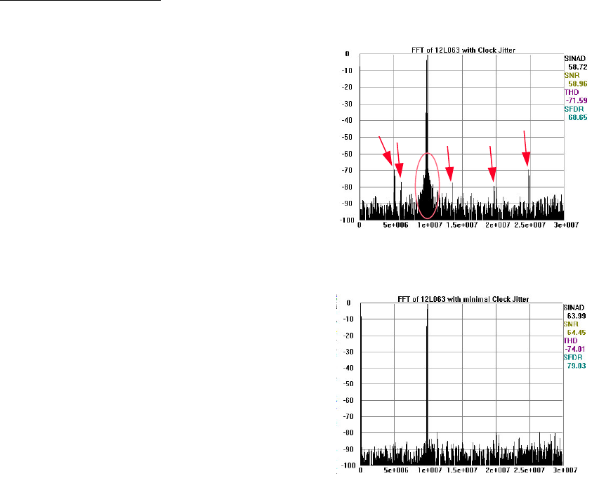
6.1 Clock Jitter
When any circuitry is added after a signal source, some
jitter is almost always added to that signal. Jitter in a
clock signal, depending upon how bad it is, can degrade
dynamic performance. We can see the effects of jitter in
the frequency domain (FFT) as "leakage" or "spreading"
around the input frequency, as seen in Figure 2a.
Compare this with the more desirable plot of Figure 2b.
Note that all dynamic performance parameters (shown to
the right of the FFT) are improved by eliminating clock
jitter.
To develop the ADC clock, WAVEVISON BRD 3.0 Digital
Interface Board divides its on-board clock to provide the
ADC clock. In doing so, jitter is introduced to the ADC
clock, degrading the observed performance of the ADC.
The amount of jitter produced by this evaluation system
is acceptable for relatively low input frequencies (below
about 5 MHz). But at higher frequencies and resolutions
this jitter can make it appear as though the ADC does not
perform well.
Figure 2a. Jitter causes a spreading around the
input signal, as well as undesirable signal spurs.
For many applications the results seen will be completely
acceptable. However, if it is desired to observe the best
results possible from the ADC, you should not use the
Digital Interface Board to capture data OR you should do
the following when using the Digital Interface Board:
1. Use an 80 MHz oscillator on the Digital Interface
Board (120 MHz for the ADC12L063) with the DIP
switches on that board set to divide the oscillator
frequency by the appropriate amount. See the
Digital Interface Board manual for details on setting
the divide ratio. The goal here is to have the divided
clock from the Digital Interface Board be the same
frequency as the oscillator on the ADC12040
Evaluation Board.
Figure 2b. Eliminating or minimizing clock jitter
results in a more desirable FFT that is more
representative of how the ADC actually performs.
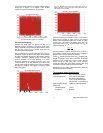
The problem of Figure 3 is obvious, but it is not as easy
to see the problem in Figure 4, where the only thing we
see is small excursions beyond the normal envelope.
Compare Figure 3 and Figure 4 with Figure 5.
2. Use a 40 MHz oscillator on the ADC12040
evaluation board, a 10 MHz oscillator for the
6 http://www.national.com