


1.0 Introduction
In the Computer mode evaluation is simplified by
connecting the board to the WaveVision Digital Interface
Board (order number WAVEVSN BRD 3.0), which is
connected to a personal computer through a serial
communication port and running WaveVision software,
operating under Microsoft Windows. Or use WAVEVSN
BRD 4.0 when available on National's web site. Use the
WaveVision2 program (WAVEVSN2.EXE) or use
WaveVision 4.0 when available on National's web site.
These Design Kits (each consisting of an Evaluation
Board, National's WaveVision software and this manual)
is designed to ease evaluation and design-in of Nationals
ADC12040, ADC12010, ADC12020, or ADC12L063 12-
bit Analog-to-Digital Converter, which operate at speeds
up to 40 Msps, 10 Msps, 20 Msps and 62 Msps,
respectively. Further reference in this manual to the
ADC12040 is meant to also include the ADC12010,
ADC12020 and the ADC12L063, unless otherwise
specified or implied. Note that the maximum sample rate
capability of the WaveVision system in the Computer or
Automatic mode is 60 Msps.
The signal at the Analog Input to the board is digitized
and is available at pins B16 through B21 and C16
through C21 of J2. Pins A16 through A21 of J2 are
ground pins.
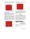
The WaveVision software can be operated under
Microsoft Windows. The signal at the Analog Input is
digitized and can be captured and displayed on a PC
monitor as a dynamic waveform. The digitized output is
also available at Euro connector J2.
Provision is made for adjustment of the Reference
Voltage, V
REF
, with VR1.
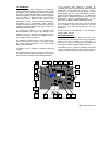
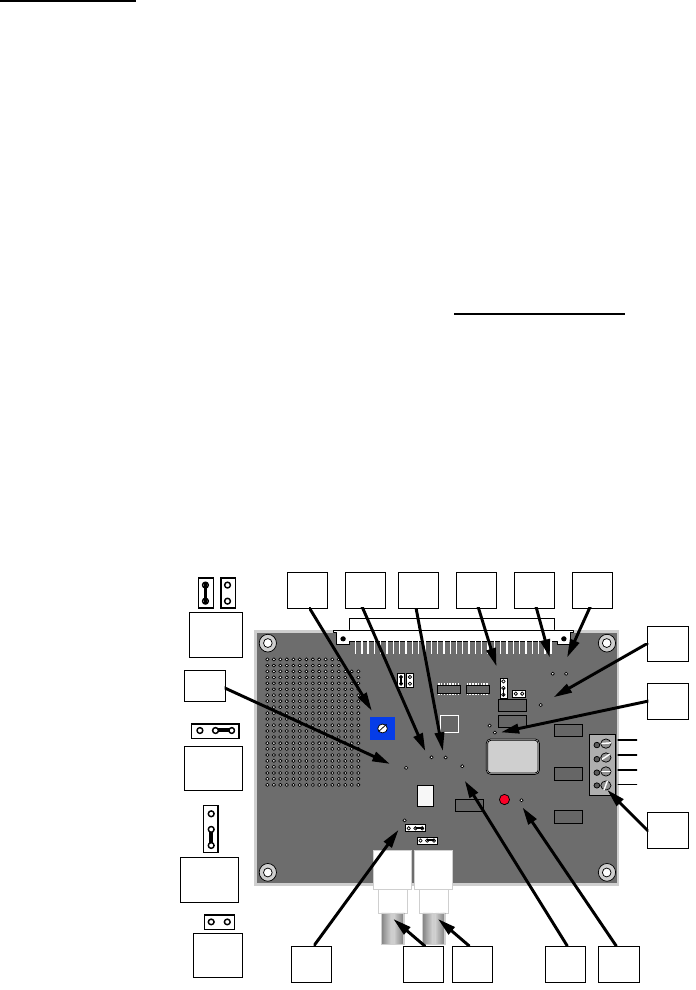
2.0 Board Assembly
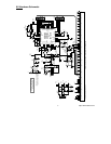
The ADC12040 Evaluation Board may come pre-
assembled or as a bare board that must be assembled.
Refer to the Bill of Materials for a description of
components, to Figure 1 for major component placement
and to Figure 6 for the Evaluation Board schematic.
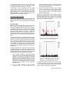
The software can perform an FFT on the captured data
upon command and, in addition to a frequency domain
plot, shows dynamic performance in the form of SNR,
SINAD, THD and SFDR.
A breadboard area is provided for building customized
circuitry. For best performance, keep circuitry neat and
arrange components to provide short, direct connections.
A prototype area is available for building customized
circuitry.
The evaluation board can be used in either of two modes.
In the Manual mode suitable test equipment can be used
with the board to evaluate the ADC12040 performance.
+V
GND
+5V
-V
Y1
L3
T1
L4
L5
L2
L10
L1
RP2 RP1
U1
CLK SEL
JP2
VR1
-V
TP10
+V
TP8
VDO
TP2
TP20
OE-
TP7
ADC CLK
Vin+
TP3
Vin-
TP4
TP6
PWR DWN
POWER CONNECTOR
P1
TP5
SIG IN
JP3
MIX
JP4
SELECT
J3 J1
VREF
TP1
+5V
TP9
D1
JS3
JS1JS0
J1
Analog
Input
VR1
Ref. Adj.
TP1
V
REF
P1
Power
TP10
-V
JP2
CLK
SELECT
TP3
Vin+
TP8
+V
TP5
SIGNAL
INPUT
TP6
PWR
DWN
TP9
+5V
JP2
Detail
Default
Position
TP4
Vin-
J3
Analog
Input
JP3 & JP4
Detail
J1 Input
Position
TP7
ADC CLK
TP2
DR VD
JS3
Detail
Standard
JS0 & JS1
Detail
Standard
Figure 1. Component and Test Point Locations
3 http://www.national.com