


CAST, Inc. 11 Stonewall Court
Woodcliff Lake, NJ 07677 USA
tel 201-391-8300 fax 201-391-8694
Copyright © CAST, Inc. 2007, All Rights Reserved.
Contents subject to change without notice.
Trademarks are the property of their respective owners.
This core developed by the
processor experts at Evatronix SA.
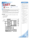
Functional Description
The CZ80CPU core is partitioned into modules as shown in
the Block Diagram and described below.
Cycle Control
The main control machine, which synchronizes all the others.
It has an instruction register and all registers controlled inter-
rupts, bus request cycle, wait states etc. This unit controls
bus control signals too.
Bus Control
Registers are triggered on the falling edge and or gates.
These are used to form the bus control timing, changed on
both clock edges. This is the only unit that has registers syn-
chronized on the falling clock edge.
Address Unit
This unit controls all operations on addresses (calculates the
next instruction address, nested data address, jump and re-
turn address etc.) and increments and decrements the 16-bit
addr register. It includes pc_reg (program counter), sp_reg
(stack pointer), i_reg (interrupt register) and r_reg (refresh
register).
NMI Control
This unit detects a falling edge on the nmin pin. If detected,
the internal nmi register is set and this causes a non-
maskable interrupt service cycle.
Reset Control
This unit controls the state of external signal resetn. If it has
value ‘0’ for at least three full clock cycles, then it sets the in-
ternal synchronous reset signal (rst) to ‘1.’
Register Bank
This includes all the commonly used registers (based and al-
ternative) and the logic element needed to change the data in
these registers.
Arithmetic-Logic Unit (ALU)
The unit accumulator and flag registers, and performs 8-bit
arithmetic and logic operations, 16-bit arithmetic operations
(without increment and decrement), bit operations, and sets
the flag register.
Implementation Results
The CZ80CPU is a technology independent design that can
be implemented in a variety of process technologies. The
following are typical Xilinx results with Fmax optimized for
speed.
Family
Fmax
(MHz)
Slices
IOB
GCLK
BRAM
MULT
DCM/
DLL
MGT
PPC
Design
Tools
Virtex-II Pro
XC2VP4-7
78
2102
38
1
0
0
0
0
0
ISE 5.2i
Virtex-E
XCV400E-8
45
2060
38
1
0
N/A
0
N/A
N/A
ISE 5.2i
Virtex-II
XC2V500-6
76
2003
38
1
0
0
0
N/A
N/A
ISE 5.2i
Spartan-IIE
XC2S300E-7
38
2388
38
1
0
N/A
0
N/A
N/A
ISE 5.2i
Spartan-3
XC3S400-4
36
1967
38
1
0
0
0
N/A
N/A
ISE 5.2i
Support
The core as delivered is warranted against defects for ninety
days from purchase. Thirty days of phone and email technic-
al support are included, starting with the first interaction.
Additional maintenance and support options are available.
Verification
The CZ80CPU core’s functionality was verified by means of a
proprietary hardware modeler. The same stimulus was ap-
plied to a hardware model that contained the original Zilog
Z84C00 chip, and the results compared with the core’s simu-
lation outputs.
Deliverables
The core is available in ASIC (synthesizable HDL) and FPGA
(netlist) forms, and includes everything required for success-
ful implementation. The Xilinx version includes:
Post-synthesis EDIF netlist
Example CZ80CHIP – 8051 compatible design. This de-
sign uses the CZ80CPU and illustrates how to build and
connect memories and port modules
Sophisticated HDL Testbench that instantiates the exam-
ple design CZ80CHIP, external RAM, external ROM, clock
generator, and process that compares your simulation re-
sults with the expected results
A collection of Z80 assembler programs which are ex-
ecuted directly by the Test Bench
Simulation script, vectors, expected results, and compari-
son utility
Place and route script
Comprehensive user documentation, including architec-
tural overview, hardware description, user guide, detailed
specifications and a system integration guide