


4.1.2 Dual Input
must be the same as that provided from the Digital
Interface Board.
To look at intermodulation performance, moving shorting
jumpers of JP3 and JP4 to pins 2 and 3 of JP3. Connect
different signals to J1 and J3 from 50-Ohm sources.
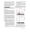
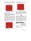
When looking at the ADC output with two different signals
at the input, the dynamic performance parameters (SNR,
SINAD, THD and SFDR) are meaningless. With two input
signals we are looking for any spurs in the frequency
domain plot (FFT). The simple method used here to mix
two signals is not adequate to completely evaluate IMD of
these converters. Consequently, the actual IMD
performance of the A/D converter is better than would be
indicated by using this method. Most high speed ADCs
exhibit high spurious content under these conditions
unless the total input swing is very low compared with full
scale.
See Section 6.1 for information on capturing data with a
clock that is not synchronized to the clock of the Digital
Interface Board.
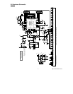
4.5 Digital Data Output
The digital output data from the ADC12040 is available at
the 96-pin Euro connector J2. Series resistors RP1 and
RP2 isolate the ADC from the load circuit to reduce noise
coupling into the ADC.
4.5 Power Supply Connections
Power to this board is supplied through power connector
P1. The only supply needed is +5V at pin 1 for the
ADC12040, ADC12010 or the ADC12020, or +3.3V at pin
1 for the ADC12L063, plus ground at pin 2 for either. Any
circuitry you breadboard may need a negative voltage at
the -V supply pin 4.
As mentioned in Section 5.0, it is important to use a
bandpass filter at BNC J1 (and BNC J3, if this input is
used) to ensure the quality of the signal presented to the
ADC and to get meaningful test results.
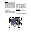
4.2 ADC reference circuitry
When using the ADC12040 Evaluation Board with the
Digital Interface Board, a 5V logic power supply for the
interface board is needed at pin 3 of P1. This supply
voltage is passed through J2 to the Digital Interface
Board.
An adjustable reference circuit is provided on the board.
The simple circuit here is not temperature stable and is
not recommended for your final design solution. When
using the resistor values shown in Figure 1, the reference
circuit will generate a nominal reference voltage in the
range of 0 to 2.4 Volts for the ADC12040, ADC12010 and
ADC12020 or 0 to 1.2 Volts for the ADC12L063. The
ADC12040, ADC12010 and ADC12020 are specified to
operate with V
REF
in the range of 1.0 to 2.4 V, with a
nominal value of 2.0V while the ADC12L063 is specified
to operate with V
REF
in the range of 0.8 to 1.2 V, with a
nominal value of 1.0V. The reference voltage can be
monitored at test point TP1 and is set with VR1.
The supply voltages are protected by shunt diodes and
can be measured at TP8, TP9 and TP10. If a
breadboarded circuit requires voltages greater than 5V,
they will have to be separately provided by the user.
4.6 Power Requirements
Voltage and current requirements for the ADC12040
Evaluation Board mode are:
For the ADC12040, ADC12010 and the ADC12020:
4.3 ADC clock circuit
• +5.0V at 100 mA [+V]
• +5.0V at 30 mA (1A when connected to the Digital
Interface Board) [+5V].
The clock signal applied to the ADC is selected with
jumper JP2. A standard crystal oscillator can be installed
at Y1 and selected with jumper JP2 pins 2 and 3 shorted
together. To use a different clock source, connect the
signal to pin B23 of J2 and select pins 1 and 2 of jumper
JP2. The ADC clock frequency can be monitored at test
point TP7. R13 and C13 are used for high frequency
termination of the clock line. In the Computer mode of
operation using the Digital Interface Board, JP2 can have
pins 1 and 2 shorted together to use the clock from the
Digital Interface Board, but this is not recommended, as
discussed in Section 6.1.
For the ADC12L063:
• +3.3V at 120 mA [+V]
• +5.0V at 30 mA (1A when connected to the Digital
Interface Board) [+5V].
There is no need for a negative supply for either ADC,
unless it may be needed for the breadboard area.
5.0 Installing the ADC12040 Evaluation Board
The evaluation board requires power supplies as
described in Section 4.6. An appropriate signal source
should be connected to the Analog Input BNC J1. When
evaluating dynamic performance, an appropriate signal
generator (such as the HP8644B, HP8662A or the R&S
SME-03) with 50 Ohm source impedance should be
connected to the Analog Input BNC J1 and/or J3 through
Note that any external clock source must have
TTL/CMOS levels. Also, if using the Digital Interface
Board from National Semiconductor to capture data, the
oscillator at Y1 should be removed, the external clock
signal supplied at pin 3 of that socket and pins 2 and 3 of
JP2 should be selected. Additionally, the clock frequency
5 http://www.national.com