


BMBMWBMWBMW
Z3
2.5 VI/SW
0110.0 INTRODUCTION
03/00
0110.0Ć
1999
00
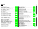
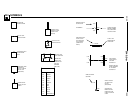
P90
FRONT POWER
DISTRIBUTION
BOX
F1
15A
GROUND
DISTRIBUTION
0670.4
6160.0-02
2.5 VI/SW
4
8
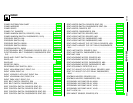
P91
REAR POWER
DISTRIBUTION
BOX
F44
30A
X293
2
6
X293
FUSE DETAILS
0670.3
4 VI/SW
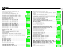
86
85
30
87
X452
CENTRAL
BODY
ELECTRONICS
(ZKE)
6100.0
K11
WIPER RELAY
FUSE DETAILS
0670.3
X493
Schematics
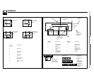
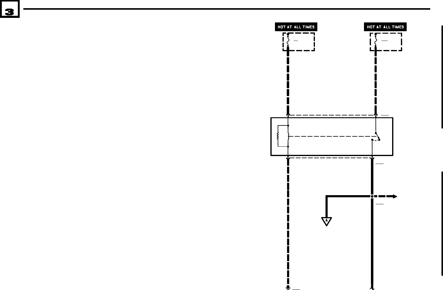
The schematics divide the entire vehicle electrical system into individual circuits. Interacting
electrical components are shown on one common schematic.
Switches and other components are represented in such a way that their general layout and
function are self–explicit. They are arranged on the sheet such that the current path can be
followed from positive (top) to negative (bottom).
Important: The components and wires are not drawn to scale. For instance, a lead with a length
of over 1m can be shown as a lead that is only a few cm long. To ensure clear arrangement , all
connectors, lines branches and connected components from the fuses to the component and
from the component to ground connection are not shown within the individual cells. If required,
reference can be made to cells 0670.3 Fuse Details and 0670.4 Ground Distribution where all
lines are illustrated with all plug connections, line branches and connected components.
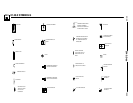
All circuit symbols used are listed and explained in cell 0140.0 Symbols.
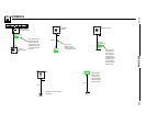
In cell 7000.0 Component Location Chart all important connectors, ground points and
components are listed in tabular form. It provides a precise description of the component
locations in the vehicle.
In cell 7100.0 Component Location Views the location of connectors and components which
are difficult to locate are shown in line arts or illustrations. In cell 8000.0 Splice Location Views
all splices are listed in numerical order and illustrations are provided to assist in locating splices
on larger harnesses. In cell 8500.0 Connector Views diagrams of connectors with more than 2
pins are illustrated.
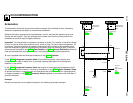
Example
General conventions can be explained based on the following schematic example.