


TMS320VC5402
FIXEDĆPOINT DIGITAL SIGNAL PROCESSOR
SPRS079E – OCTOBER 1998 – REVISED AUGUST 2000
1
POST OFFICE BOX 1443 • HOUSTON, TEXAS 77251–1443
D Advanced Multibus Architecture With Three
Separate 16-Bit Data Memory Buses and
One Program Memory Bus
D 40-Bit Arithmetic Logic Unit (ALU),
Including a 40-Bit Barrel Shifter and Two
Independent 40-Bit Accumulators
D 17- × 17-Bit Parallel Multiplier Coupled to a
40-Bit Dedicated Adder for Non-Pipelined
Single-Cycle Multiply/Accumulate (MAC)
Operation
D Compare, Select, and Store Unit (CSSU) for
the Add/Compare Selection of the Viterbi
Operator
D Exponent Encoder to Compute an
Exponent Value of a 40-Bit Accumulator
Value in a Single Cycle
D Two Address Generators With Eight
Auxiliary Registers and Two Auxiliary
Register Arithmetic Units (ARAUs)
D Data Bus With a Bus-Holder Feature
D Extended Addressing Mode for 1M × 16-Bit
Maximum Addressable External Program
Space
D 4K x 16-Bit On-Chip ROM
D 16K x 16-Bit Dual-Access On-Chip RAM
D Single-Instruction-Repeat and
Block-Repeat Operations for Program Code
D Block-Memory-Move Instructions for
Efficient Program and Data Management
D Instructions With a 32-Bit Long Word
Operand
D Instructions With Two- or Three-Operand
Reads
D Arithmetic Instructions With Parallel Store
and Parallel Load
D Conditional Store Instructions
D Fast Return From Interrupt
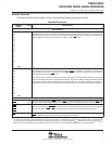
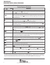
D On-Chip Peripherals
– Software-Programmable Wait-State
Generator and Programmable Bank
Switching
– On-Chip Phase-Locked Loop (PLL) Clock
Generator With Internal Oscillator or
External Clock Source
– Two Multichannel Buffered Serial Ports
(McBSPs)
– Enhanced 8-Bit Parallel Host-Port
Interface (HPI8)
– Two 16-Bit Timers
– Six-Channel Direct Memory Access
(DMA) Controller
D Power Consumption Control With IDLE1,
IDLE2, and IDLE3 Instructions With
Power-Down Modes
D CLKOUT Off Control to Disable CLKOUT
D On-Chip Scan-Based Emulation Logic,
IEEE Std 1149.1
†
(JTAG) Boundary Scan
Logic
D 10-ns Single-Cycle Fixed-Point Instruction
Execution Time (100 MIPS) for 3.3-V Power
Supply (1.8-V Core)
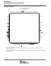
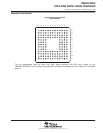
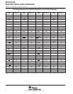
D Available in a 144-Pin Plastic Low-Profile
Quad Flatpack (LQFP) (PGE Suffix) and a
144-Pin Ball Grid Array (BGA) (GGU Suffix)
NOTE:This data sheet is designed to be used in conjunction with the
TMS320C5000 DSP Family Functional Overview
(literature number SPRU307).
Please be aware that an important notice concerning availability, standard warranty, and use in critical applications of
Texas Instruments semiconductor products and disclaimers thereto appears at the end of this data sheet.
Copyright 2000, Texas Instruments Incorporated
†
IEEE Standard 1149.1-1990 Standard-Test-Access Port and Boundary Scan Architecture.
PRODUCTION DATA information is current as of publication date.
Products conform to specifications per the terms of Texas Instruments
standard warranty. Production processing does not necessarily include
testing of all parameters.