


Transistors
1
Publication date: April 2003 SJC00230BED
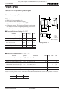
2SD1824
Silicon NPN epitaxial planar type
For low-frequency amplification
■ Features
• High forward current transfer ratio h
FE
• Low collector-emitter saturation voltage V
CE(sat)
• High emitter-base voltage (Collector open) V
EBO
• S-Mini type package, allowing downsizing of the equipment
and automatic insertion through the tape packing and the maga-
zine packing.
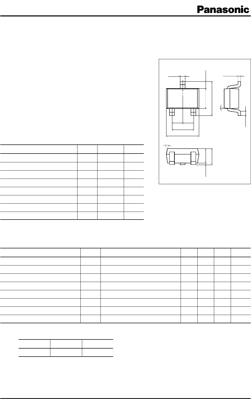
■ Absolute Maximum Ratings T
a
= 25°C
Parameter Symbol Rating Unit
Collector-base voltage (Emitter open) V
CBO
100 V
Collector-emitter voltage (Base open) V
CEO
100 V
Emitter-base voltage (Collector open) V
EBO
15 V
Collector current I
C
20 mA
Peak collector current I
CP
50 mA
Collector power dissipation P
C
150 mW
Junction temperature T
j
150 °C
Storage temperature T
stg
−55 to +150 °C
Parameter Symbol Conditions Min Typ Max Unit
Collector-base voltage (Emitter open) V
CBO
I
C
= 10 µA, I
E
= 0 100 V
Collector-emitter voltage (Base open) V
CEO
I
C
= 1 mA, I
B
= 0 100 V
Emitter-base voltage (Collector open) V
EBO
I
E
= 10 µA, I
C
= 015V
Collector-base cutoff current (Emitter open)
I
CBO
V
CB
= 60 V, I
E
= 0 0.1 µA
Collector-emitter cutoff current (Base open)
I
CEO
V
CE
= 60 V, I
B
= 01µA
Forward current transfer ratio
*
h
FE
V
CE
= 10 V, I
C
= 2 mA 400 1
200
Collector-emitter saturation voltage V
CE(sat)
I
C
= 10 mA, I
B
= 1 mA 0.05 0.20 V
Transition frequency f
T
V
CB
= 10 V, I
E
= −2 mA, f = 200 MHz 90 MHz
■ Electrical Characteristics T
a
= 25°C ± 3°C
Unit: mm
Note) 1. Measuring methods are based on JAPANESE INDUSTRIAL STANDARD JIS C 7030 measuring methods for transistors.
2.
*
: Rank classification
2.1
±0.1
1.3
±0.1
0.3
+0.1
–0.0
2.0
±0.2
1.25
±0.10
(0.425)
1
3
2
(0.65)
(0.65)
0.2
±0.1
0.9
±0.1
0 to 0.1
0.9
+0.2
–0.1
0.15
+0.10
–0.05
5°
10°
1: Base
2: Emitter
3: Collector
EIAJ: SC-70
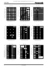
SMini3-G1 Package
Rank R S
h
FE
400 to 800 600 to 1
200
Marking symbol: 1V
This product complies with the RoHS Directive (EU 2002/95/EC).